Characterization of Thin GaN Layers Deposited by Hydride Vapour Phase Epitaxy (HVPE) on 6H- SiC Substrates
- PDF / 1,153,623 Bytes
- 6 Pages / 612 x 792 pts (letter) Page_size
- 40 Downloads / 398 Views
Characterization of Thin GaN Layers Deposited by Hydride Vapour Phase Epitaxy (HVPE) on 6HSiC Substrates J.T. Wolan,1 Y. Koshka, S.E. Saddow,2 Yu. V. Melnik3, and V. Dmitriev3 1
Dave C. Swalm School of Chemical Engineering, Mississippi State, MS 39762-9595 Emerging Materials Research Laboratory, Department of Electrical & Computer Engineering, Mississippi State, MS 39762-9571 3 TDI, Inc., Gaithersburg, MD, 20877 2
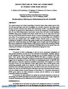
Abstract In this study, the near-surface regions of air-exposed thin GaN layers deposited by hydride vapour phase (HVPE) epitaxy on 6H-SiC substrates have been examined. Chemical-state identification and in-depth elemental distribution profiles are evaluated using angle-resolved X-ray photoelectron spectroscopy (ARXPS) and secondary ion mass spectroscopy (SIMS). The epilayers show a high degree of chemical purity as determined by XPS and SIMS. Low temperature photoluminescence (PL) were performed and is dominated by donor-acceptor pairs (DAP) emission. Layer thickness was measured to be ~ 600-700 nm and an abrupt, well-defined heterointerface is observed using scanning electron microscopy (SEM) and SIMS. Introduction The group III nitrides (AlN, GaN and IN) represent an important triad of materials due to their direct band gaps that span the entire visible region and extend well into the ultraviolet range. GaN-based high-brightness blue and white (using blue excitation of phosphors) light emitting diodes (LEDs) are commercially available [1] and blue laser diodes (LDs) have been demonstrated [2]. Despite this impressive progress, the lack of a suitable GaN substrate that is both lattice- matched and thermally compatible has hindered the development of III-V nitride devices. Ideally, bulk GaN crystals would be used for substrates; however, those currently available do not exceed a few millimeters in size. SiC is an attractive substrate for epitaxial growth of GaN films exhibiting excellent lattice and thermal compatabilities. Due to high SiC thermal conductivity (~ 4 W/cm-K) and cleavage possibilities, this system is particularly attractive for high-power electronic and photonic applications. This is due, in part, to their attractive material properties such as, high breakdown fields, high thermal conductivity; highsaturated electron velocities and large electron mobilities [3-6]. In addition, the use of SiC in this hybrid design will benefit from current silicon carbide technology already under development and the unique high-temperature and power properties of the material. GaN n-type layers were grown by HVPE on n-type 6H-SiC manufactured by Cree Research, Inc. The layers were deposited on the on-axis (0001)Si face of 41 mm diameter substrates. The GaN layers were directly deposited on the SiC substrates without a buffer layer. A hot-wall open flow horizontal reactor using an Ar carrier gas was employed. HCl (g) flows over a liquid Ga source forming GaCl (g) that is then transported to the growth zone and reacted with NH3 resulting in GaN deposition on the SiC substrate. Growth rates and temperatures w
Data Loading...