Chemical Fluid Deposition Enables Conformal Coating of High-Aspect-Ratio Features in Si Wafers
- PDF / 45,931 Bytes
- 1 Pages / 612 x 792 pts (letter) Page_size
- 41 Downloads / 362 Views
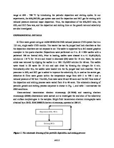
Chemical Fluid Deposition Enables Conformal Coating of HighAspect-Ratio Features in Si Wafers The increasing miniaturization of microelectronic devices has put heavy demands on the technologies used to produce them. For example, as the width of interconnect features in integrated circuits approaches 100 nm, conventional deposition techniques may be insufficient to uniformly fill these high-aspect-ratio channels with copper. Current Cu metallization techniques based on electrolytic plating require a conformal seed layer prior to feature fill. These seed layers are deposited using lineof-sight physical vapor deposition techniques that become limited in small, highaspect-ratio features. An alternative is to use chemical vapor deposition (CVD). The relatively low vapor pressures of the organometallic precursors used in CVD, however, produce mass-transport limitations that can lead to nonuniform deposition of metal in the channels, resulting in faulty connections between functional devices on a chip. To overcome these limitations, researchers at the University of Massachusetts have developed a technique called chemical fluid deposition (CFD), which involves organometallic precursors dissolved in supercritical CO2 (sc-CO2). As reported by J. Blackburn and co-workers in the October 5 issue of Science, CFD provides a precursor concentration of up to 3 orders of magnitude greater than CVD, while maintaining transport properties that are similar to those of a gas; this combination allows rapid diffusion of the organometallic into the narrow channels, promoting a uniform conformal coating. The addition of hydrogen gas, which is miscible in sc-CO2, then reduces the precursor to its metallic state, the researchers said. Silicon test wafers were placed in a coldwalled high-pressure reactor vessel at a pressure of 200 atm. The silicon substrate was resistively heated to temperatures ranging from 175°C to 200°C in sc-CO2 solutions containing Cu(II) bishexafluoroacetylacetonate [Cu(hfac)2] or Cu(II) tetramethylheptanedionate [Cu(tmhd) 2 ]. Copper was deposited by hydrogen reduction exclusively on Ni films or small Pd seed clusters. By raising the temperature to 250°C, the researchers were able to deposit metallic Cu from Cu(tmhd)2 directly onto the native silicon oxide surface in a single step, without the need for seed crystals. Cu(tmhd)2 provides the option of a nonfluorinated precursor, which reduces environmental concerns, according to the research team. The deposited films were continuous, highly reflective, and essentially free of impurities. 970
The researchers also deposited nickel onto Pd seed clusters from a solution of bis(cyclopentadienyl)nickel (NiCp2) in scCO2 in a hot-walled reactor at 60°C and 200 atm in the presence of hydrogen. They said that raising the temperature to 120°C eliminated the need for seed clusters. For both Cu and Ni, scanning electron microscopy images revealed conformal coating of 100-nm-wide by 800-nm-deep channels etched in silicon wafers, the researchers said. Furthermore, they said, secondary
Data Loading...