Chemical Vapor Deposition and Defect Characterization of Silicon Carbide Epitaxial Films
- PDF / 2,035,149 Bytes
- 6 Pages / 595 x 842 pts (A4) Page_size
- 33 Downloads / 454 Views
0891-EE12-11.1
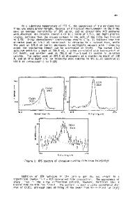
Chemical Vapor Deposition and Defect Characterization of Silicon Carbide Epitaxial Films Yi Chen, Govindhan Dhanaraj, Hui Chen, William Vetter and Michael Dudley Department of Materials Science and Engineering Hui Zhang Department of Mechanical Engineering Stony Brook University Stony Brook, NY 11794-2275 ABSTRACT SiC homo-epitaxial layers have been grown using a halide chemical vapor deposition (HCVD) process. The thermodynamic process of SiC CVD in SiCl4-C3H8-H2 gas system was studied using equilibrium model. The predicted growth rate decreases gradually with the increase in growth temperature, and this trend is consistent with our experimental results. Good quality epitaxial layers with low density of basal plane dislocations could be grown. Some elementary screw dislocations present in the substrate do not seem to be propagating into the epitaxial layer. INTRODUCTION Silicon carbide (SiC) wide band-gap semiconductor is an excellent material for certain critical applications due to its unique combination of electronic and physical properties [1-3]. Chemical vapor deposition (CVD) is the most widely used technique to grow epitaxial layers for the semiconductor device fabrication [4]. SiC epitaxial layer of about 100 µm or more is needed for the high voltage rectifier device, which demands a higher growth rate for cost effective production [5]. CVD epitaxial layers grown at 1600ºC using silane and propane have a very low growth rate of 3-15 µm/hr. It is possible to grow thick epitaxial layers with very low defect densities using silicon tetrachloride (SiCl4) because of its lower decomposition temperature over the conventional silane. Recently, halide CVD (HCVD) was developed as an alternative to the high temperature CVD to achieve higher growth rate at relatively lower temperature [6,7]. However, nucleation of defects such as hollow-core dislocations (also know as micropipes or MPs) and process induced basal plane dislocations remains as big challenge in SiC devices fabrication [8-10]. Synchrotron white beam X-ray topography can easily reveal most of the structural defects present in the substrate as well as in the epitaxial layer [10,11]. Recently developed growth assisted hydrogen defect etching can also be used to record MPs [12]. Better understanding on the growth process and defect nucleation is needed for optimizing the epitaxial growth to obtain high quality layers. EXPERIMENTAL DETAILS Epitaxial films were grown in our home-made CVD system [13] using silicon tetrachloride (SiCl4) and propane (C3H8) as silicon and carbon precursors, respectively. Hydrogen was used as the carrier gas. The schematic diagram of the CVD epitaxial growth system containing gas cabinets, flow controllers and hot zone is shown in Fig. 1. Numerical
0891-EE12-11.2
modeling was used to obtain the temperature field in the hot-zone [13]. Hydrogen was bubbled through silicon tetrachloride liquid contained in the temperature and pressure controlled source bottle, and the hydrogen gas saturated with SiCl4 vapors was passe
Data Loading...