Comparison of Current and Light Induced Defects in A-SI:H
- PDF / 296,083 Bytes
- 6 Pages / 414.72 x 648 pts Page_size
- 109 Downloads / 343 Views
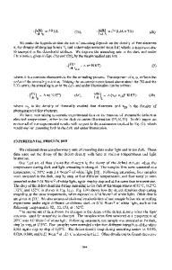
COMPARISON OF CURRENT AND LIGHT INDUCED DEFECTS IN A-SI:H R. A. STREET, W. B. JACKSON AND M. HACK Xerox Palo Alto Research Center, Palo Alto, CA 94304 ABSTRACT Metastable defect creation by illumination and by a forward current in p-i-n devices are compared using CPM and reverse current measurements of the defect density. The data show that the same defects are formed by the two mechanisms, but with different spatial profiles. Numerical modelling shows how the spatial profile influences the reverse bias current. INTRODUCTION Both prolonged illumination and a forward bias current cause a metastable increase in the defect density of a-Si:H and the degradation of p-i-n solar cells. There is good reason to expect that the same defects are formed because both mechanisms generate electrons and holes which cause defect creation by recombination. However, there have been a few suggestions that current-induced and light-induced defects are different. For example, Kida et al report that both mechanisms increase in the sub-gap absorption while only light-induced defects reduce the carrier trapping [11, while Gunes and Wronski report differences between annealed and light-induced defects [2]. This paper presents experiments and numerical modelling which compare defect generation by illumination and forward current on the same sample. Measurements were made of the subgap absorption and of the reverse bias current, both of which yield a measure of the defect density. A numerical computer model is used to analyse the reverse bias current.
10-1
10-2
Absorption (arb units)
10-3 10-4
.5
1 1.5 Energy (eV)
2
Fig. 1. CPM data showing the increase of the sub-gap absorption after current-induced defect formation. The Urbach edge region is unchanged. Mat. Res. Soc. Symp. Proc. Vol. 297. ©1993 Materials Research Society
554
EXPERIMENTAL RESULTS The samples used are n-i-p diodes of thickness 1.2 pm and area 4 mm2 . Light soaking was performed with a tungsten lamp focussed to an intensity of about 1 W/cm 2 , with filters to remove blue and infra-red light. Current soaking was performed at 0.1 A/cm 2 , which required a voltage of about 2V. The CPM measurements were made with the sample under a reverse bias of 1V and a photocurrent of 3x10-11 A. The data are presented without any correction to remove interference fringes. Reverse bias measurements of the dark leakage current were made at 1V bias after the current had decayed for 5 minutes to allow for charge depletion from the sample [3]. Current-voltage (J-V) data were acquired with a delay of 2 minutes between each voltage increment. CPM data Figure 1 shows examples of the CPM data for a sample in the annealed and various current-soaked states. The sub-gap absorption increases after defect generation and the Urbach edge slope is unchanged, as found for the light-soaked samples. There is an order of magnitude increase in the defect density as compared to the annealed state, which is typical of other degradation measurements. Differences in the shape of the defect absorption bands w
Data Loading...


