Conductance Transients Study of Slow Traps in Al/SiN x :H/Si and Al/SiN x :H/InP Metal-Insulator-Semiconductor Structure
- PDF / 394,127 Bytes
- 6 Pages / 414.72 x 648 pts Page_size
- 67 Downloads / 283 Views
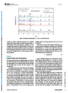
EXPERIMENT Sample Preparation The devices were obtained as follows: Substrates used were n-type silicon wafers with a resistivity of 5 Licm, and unintentionally doped n-type InP wafers (5x 10i 5 cm 3 ) respectively. Prior to the insulator deposition, back electrodes were deposited by thermal evaporation of aluminum on silicon and an AuGe/Au alloy on InP wafers. After this, the wafers were cleaned with organic solvents and, then, the native oxides were stripped in a solution of H20:HF, followed by a 3 min. rinse in deionized water and drying in N2. Then they were transferred to the insulator deposition chamber: a vacuum chamber of our design attached to an ECR reactor (Astex 4500). Substrate temperature (200 °C) and total pressure (0.6 mTorr) were kept constant in all the experiments. Microwave power was varied in the range 50-200 W for silicon wafers and was kept constant (100 W) for the InP samples. Gases used were N2 to generate the plasma and pure Sil4. The value of the gases flux ratio [N2]/[SiH 4] was varied from I (x=0.91) to 9 (x=1.49) for the two types of semiconductor wafers. The deposition time was scaled to obtain insulator film thickness of 500kA. Finally, Al dots (1.2x10- 3 cm 2) were thermally evaporated with a mechanical mask and post metallization annealing was conducted in inert atmosphere. Electrical Characterization The electrical characteristics of the semiconductor/insulator interfaces are similar to those using passivation layers. In the case of films deposited over silicon, we observe that better values of the electrical properties are obtained for near stoichiometric films and poor values were obtained for both Sirich and N-rich films. We used the C-V technique to determine the existence of traps in the insulatorsemiconductor interface. The interface state density existing in these structures was kept in the range (35)x10 1 cm-2 eV' for films with [N]/[Si] ratio lower than 1.38. For nitrogen rich films, the trap density suddenly increases following the same trend as the concentration of N-H bonds in the SiNx :H film. This result is explained on the basis of the model reported by Lucovsky et al. [7] for Oxide-Nitride-Oxide/Si structures. The model is additionally supported by DLTS measurements (Fig. 1) that show the presence of silicon dangling bonds at the insulator/semiconductor interface (the so called PbNO centers). The concentration of these centers depends on the insulator composition in a similar way as the interface trap density and, i.e., as the N-H bond concentration. Moreover, this result supports the assumption that the N-H bonds located at the interface act as precursor of eSi-Si 3 type defects, that is, of PbNO centers. In conclusion, a close relation between interface trap density, PbNO centers and N-H bond density can be established. As for the films deposited on InP, the C-V and DLTS results (Fig.2) suggest an inverse correlation between the insulator composition and the density of interface traps. The minimum trap density concentration (2x 1012 cm 2 eV' at 0.32 eV above the mi
Data Loading...