Control of Amorphous Silicon Crystallization Using Germanium Deposited by Low Pressure Chemical Vapor Deposition
- PDF / 547,913 Bytes
- 6 Pages / 612 x 792 pts (letter) Page_size
- 89 Downloads / 381 Views
Control of Amorphous Silicon Crystallization Using Germanium Deposited by Low Pressure Chemical Vapor Deposition Masato Toita1, Pranav Kalavade and Krishna C. Saraswat Department of Electrical Engineering, Stanford University, Stanford, CA 94305-4070 1 Asahi Kasei Microsystems Co. Ltd., Tokyo 151-0053, JAPAN ABSTRACT Crystallization behavior of 100nm amorphous silicon film with and without a 160nm poly-Ge layer on top was investigated. Ge was observed to increase the nucleation rate as well as to increase the incubation time for nucleation in a-Si. Activation energy for nucleation was 2.3eV for Ge-covered Si films as compared to 2.7eV for the control a-Si films with no poly-Ge. Activation energy for incubation is almost unchanged for both the films (-3.3eV). An alternative seeding technique for a-Si films using the increase in the incubation time for nucleation due to presence of poly-Ge is proposed. INTRODUCTION Polysilicon thin film transistors (poly-Si TFT's) are widely used as pixel switching devices on active matrix liquid crystal displays (AMLCD's). High performance poly-Si TFT's are also attractive for three-dimensional (3-D) circuit applications [1]. Solid phase crystallization (SPC) of amorphous silicon is a promising method to fabricate high performance poly-Si TFT's that can be applied for 3-D integrated circuits. Submicron TFT’s suffer from performance variations caused by statistical variation in the number of grains within the channel [2]. Therefore, a control over grain locations in SPC silicon thin films is particularly desirable to realize 3-D circuit applications. Several seeding techniques to obtain control over grain locations were demonstrated. To achieve the spatially controlled crystallization of amorphous silicon, the seeding agent is placed in the designated region (seed hole) to promote nucleation at the region. This is followed by a thermal annealing step to grow the crystal grain laterally from the seeded region to the adjacent unseeded region to be used as a channel film for TFT’s. Metal induced lateral crystallization (MILC) is one such seeding technique, in which metal, such as nickel, is used as the seeding agent for a-Si crystallization [3]. Germanium can also be used as a seeding agent for spatially controlled crystallization of a-Si [4]. Since metals such as nickel have detrimental effect on device performance [5], Ge seeding technique has much better compatibility to scaled CMOS technology.
A9.5.1
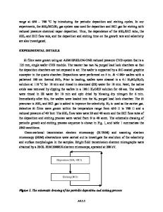
Typical process flow of Ge seeding Amorphous Silicon Deposition technology is schematically shown in Figure Amorphous Silicon (a) 1. In this sequence, an amorphous silicon SiO 2 layer is deposited on oxidized silicon Masking Oxide (LTO) Deposition substrates (a); the surface of a-Si is covered Seed Hole Patterning LTO with a masking SiO2 layer and seed holes are opened (b); poly-Ge is then selectively Amorphous Silicon (b) deposited in the seed holes and is an excellent seeding agent for SPC of a-Si (c). Subsequent annealing results in nucleation Selective Deposition of Germanium and
Data Loading...