Low Temperature Silicon Nitride Films Deposited on 3D Topography by Hot Wire Chemical Vapor Deposition (HWCVD)
- PDF / 519,266 Bytes
- 6 Pages / 612 x 792 pts (letter) Page_size
- 8 Downloads / 448 Views
1036-M03-01
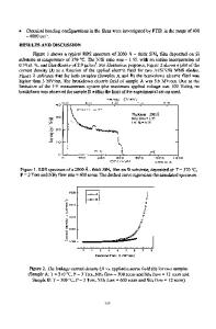
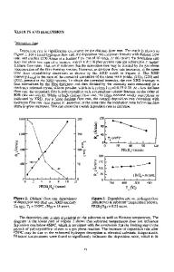
Low Temperature Silicon Nitride Films Deposited on 3D Topography by Hot Wire Chemical Vapor Deposition (HWCVD) Stephan Warnat1, Markus Hoefer2, Lothar Schaefer2, Helmut Foell3, and Peter Lange1 1 Fraunhofer Institute for Silicon Technology, Itzehoe, 25524, Germany 2 Fraunhofer Institute for Surface Engineering and Thin Films, Braunschweig, 38108, Germany 3 Technical Faculty, Christian-Albrechts-University, Kiel, 24143, Germany ABSTRACT Silicon nitride films were deposited by hot-wire chemical vapor deposition processes (HW-CVD). The films reveal a morphological structure very similar to nitrides formed in low pressure CVD (LP-CVD) or plasma enhanced CVD (PE-CVD) processes. The electrical breakdown voltages, however, are much smaller for HW- than PE- or LPCVD films. The deposition in holes for isolation purpose in “through silicon vias” (TSV) was investigated. The integration with optical devices require very low temperatures (20 nm thick films also at rough surfaces the required voltage stability against breakthrough events will be fulfilled for the planned application. Film thickness measurements inside 300 µm deep holes have shown that 30 nm thick films can be deposited in the holes by the HW-CVD technique. Further investigations must show if the film stoichiometry inside the film is comparable to the planar investigation. However, the HW-CVD technique is therefore viewed as a tentative deposition method for SiN-films inside TSV.
Figure 3: The left figure shows a measured profiles of SiN-film thickness deposited by HWCVD and PE-CVD as a function of the hole depth . The right figure shows a SEM pictures of an HW-CVD SiN-film at the bottom of the 300 µm deep hole.
ACKNOWLEDGMENTS The authors would like to thank the German Ministry of Education and Science for their financial support in the BMBF project “micro camera”. REFERENCES [1] [2] [3] [4] [5] [6] [7] [8]
H. Matsumura, "Method for Depositing a Thin Film," vol. 6,069,094, N. Corporation and A. Corporation, Eds. USA: Hideki Matsumura, 2000, pp. 11. S. Warnat, N. Marenco, D. Kähler, and W. Reinert, "Design rules for post-CMOS through silicon vias in an industrial environment," presented at 8th Electronic Packaging Technology Conference, Singapore, 2006. G. Barbottin and A. Vapaille, Instabilities in Silicon devices, vol. I: North-Holland, 1986. H. Matsumura, "Summary of research in NEDO Cat-CVD project in Japan," Thin Solid Films, vol. 395, pp. 1-11, 2001. P. Lange, "Evidence for disorder-induced vibrational mode coupling in thin amorphous SiO2 films," Journal of Applied Physics, vol. 66, pp. 201, 1989. D. V. Tsu, G. Lucovsky, and M. J. Mantini, "Local atomic structure in thin films of silicon nitride and silicon diimide produced by remote plasma-enhanced chemical-vapor deposition," Physical Review B, vol. 33, pp. 7069, 1986. C. M. M. Denisse, K. Z. Troost, F. M. P. M. Habraken, W. F. v. d. Weg, and M. Hendriks, "Annealing of plasma silicon oxynitride films " Journal of Applied Physics, vol. 60, pp. 2543, 1986. E. Fuchs, H. Oppolzer, and H. Rehme,
Data Loading...