Control of Sizes and Optical Emission of Sige Quantum Dots Prepared on Ordered Mesoporous Silica Coated Si Wafer
- PDF / 1,631,849 Bytes
- 6 Pages / 414.72 x 648 pts Page_size
- 94 Downloads / 271 Views
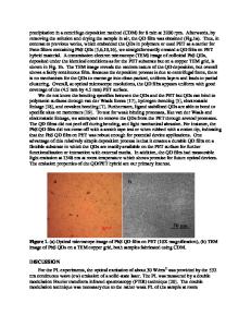
media, any over-saturated Ge growth on top of the buried dot array tends to form a second set of larger dot array, which has also a very high density and dot size uniformity. The samples were then studied by Atomic Force Microscope (AFM), double axis X-ray diffraction, Raman and low temperature photoluminescence spectroscopy. RESULTS AND DISCUSSION AFM Examination AFM was used to examine the surface morphology of both the silica substrate and the SiGe coated sample. Typical results are shown in Fig.l. The pores in the silica film before SiGe growth (Fig.la) are not very clear due to the fact that they are filled with C-Br compounds, which become volatile gas species when heated at above 300C, while Fig.lb shows the existence of a very high density top dot array. Further cross-section scanning electron microscopic examination of the same sample suggests that at least some of the SiGe have been introduced into the pores.
!A
(a) AFM image of "wet" silica surface (b) AFM image of a Si0.5Ge0 .5 dot sample Fig.1 AFM pictures of the top surface of (a) a silica coated substrate and (b) a Si 0.5Ge0 .5 dot sample after heat treatment at 500C for 90min. The unclear pores on the silica coated substrate (a) are due to the filling of C-Br compounds, which will escape when heated at above 300C
In addition to the possible buried nanostructures inside the silica matrix, AFM examination also gives us information on the dependence of the top dot sizes on the MBE SiGe thickness (Fig.2). It was found that the size of the top layer dots linearly depends on the thickness of the SiGe layer we grow, and the sizes of the top dots do not vary with further post-growth thermal anneal. This enables us to have two different controllable sizes of dots formed simultaneously, the buried dot size controlled by the surfactant and the top dot size controlled by the growth. X-Ray Diffraction In order to check whether the SiGe has formed layered arrays, double axis X-ray diffraction (XRD) was performed on a Crystal Logic powder diffractometer using the 1.125 kW copper K-al X-ray source and a graphite monochromator. Shown in Fig.3 is a comparison of the XRD of a Si0.5 Ge0.5 quantum dot sample and a "wet" silica coated Si substrate in the same region corresponding to the structures in the silica layers. It can be found that the dot sample has clear observable diffraction satellites up to the second order centered at around 23.65 degrees off the (004) direction of the Si substrate peak, suggesting the formation of buried layers of SiGe in the sample. The weaker XRD peak from the substrate might be due to that the dot sample had subjected to high temperature heat during and after the MBE growth, which reduced the silica coating thickness. Further XRD studies are in progress in order to confirm the observation. Assuming this diffraction pattern comes from the buried dots inside the mesoporous silica matrix, the inter-layer separation may be dominantly decided by the layered tube-like pores which are arranged in such a way that the openings of these pores a
Data Loading...