Control of Stress in Surface Engineered Silicon
- PDF / 655,247 Bytes
- 6 Pages / 612 x 792 pts (letter) Page_size
- 10 Downloads / 357 Views
T4.8.1
Control of Stress in Surface Engineered Silicon Y. Ma, R. Job, B. Zölgert, W. Düngen, Y. L. Huang, W.R. Fahrner University of Hagen (LGBE), P.O. Box 940, D-58084 Hagen, Germany
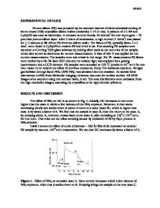
ABSTRACT Hydrogen plasma (H-plasma) treatments applied on (100)-oriented standard Czochralski (Cz) silicon wafers cause a structuring of the surface regions in the sub-100 nm scale. The reconstruction of the ‘nano-structured’ surface layers by high temperature vacuum annealing induces strong tensile stress (~ GPa) at the surface and in the subsurface regions of the wafers, as can be verified by depth resolved µ-Raman spectroscopy (µRS). Although the H-plasma caused ‘nano-structured’ surface layer is very thin (100 – 200 nm), the stressed subsurface regions of the annealed samples are quite extended, i.e. up to ∼ 10 µm depth. The impacts of several process parameters including 1) the doping type of the wafer substrate, 2) the frequency of the H-plasma, 3) the power and duration of the H-plasma, 4) the temperature and duration of the vacuum annealing on the stress are investigated. It is found that the stressed region in the surface engineered silicon wafer can be controlled by the process parameters. The presented results might be important for various applications in semiconductor technology. For example, the Hplasma exposure could be done in local areas near the electrically active regions on the forefront of the wafer. After appropriate annealing, stressed local regions for external getter purposes can be created. Such a method might especially be useful for the formation of getter regions on SOI substrates. INTRODUCTION It is well known that hydrogen plays an important role in modern semiconductor industry and has prompted many experimental and theoretical studies on this subject since the last three decades [1-3]. The presence of hydrogen can seriously alter the properties of the semiconductor material such as passivating shallow and deep level impurities, catalyzing thermal donor formation (see [3] and references quoted therein), and facilitating the smart-cut® process [4]. Our recent investigations concentrate on the development of environmentally friendly, low cost and low thermal budget processes taking advantage of some catalytic properties of hydrogen in silicon. For such investigations hydrogen is incorporated into silicon wafers by H-plasma treatments at moderate temperatures (~ 260 °C). Due to its high activity, a hydrogen exposure causes a strong impact on the treated Cz silicon substrates. The hydrogen related effects on the Cz silicon wafers can be separated into either surface, subsurface or bulk effects depending on the local regions, where the hydrogen caused actions occur, i.e., a three-layer structure of the Hplasma treated wafers can be defined [5]. Our previous investigations have revealed that H-plasma treatments applied on the Cz silicon wafers cause a structuring of the surface regions in the sub-100 nm scale. The reconstruction of the ‘nano-structured’ surface layers by high temperature annealing induces st
Data Loading...