Copper Films Prepared by Metal Organic Chemical Vapor Deposition (MOCVD) Process Using Copper (Acetylacetonate) and Wate
- PDF / 1,041,160 Bytes
- 6 Pages / 420.48 x 639 pts Page_size
- 34 Downloads / 381 Views
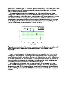
COPPER FILMS PREPARED BY METAL ORGANIC CHEMICAL VAPOR DEPOSITION (MOCVD) PROCESS USING COPPER (ACETYLACETONATE) AND WATER VAPOR AS REACTANTS: THE IMPACT OF WATER VAPOR Yu-neng Chang Center for Interfacial Materials and Crystallization Department of Chemical Engineering Iowa State University, Ames, IA 50010 ABSTRACT By using the strong reductive potential of copper acetylacetone (Cu(acac) 2) when Cu(acac) 2) was thermally decomposed, copper metal films were prepared by metal organic chemical vapor deposition (MOCVD) process using sublimed Cu(acac)2 vapor and water vapor as reactants, at one atmosphere pressure. According to thermodynamic calculations, Cu films could be prepared by MOCVD process with a high ratio of partial pressures for water vapor and Cu(acac) 2 vapor (PH20OPCu(ac)2> 3 0). In this paper, the impacts of MOCVD processing parameters such as water vapor partial pressure, total carrier gas flow rate, and precursor partial pressure on film composition and microstructure were investigated. Deposition temperature is the primary processing parameter affecting film stoichiometry. In a specific deposition temperature window, from 370oC to 4000C, polycrystalline Cu films with Cu [1111 preferential orientation were deposited. IR and XRD results indicated that films deposited at temperature lower than 350C(2 contain copper oxide phase with poor crystal structure. By comparing the values of X-ray Auger Electron Spectroscopy (XAES) and Auger parameter (aAu) from photoelectrons of Cu films and standards from reference compounds, the principle oxidation state of copper in these films was determined as Cu(0). The deposition results indicated that a water vapor partial pressure above 10 torr is necessary to produce Cu films. As indicated by SEM, Increasing the carrier gas flow rate, above 600 sccm, can reduce the average temperature profile in the thermal boundary layer above the substrate surface, retard the gas phase reaction rate, presumably eliminate the homogeneous nucleation, and deposit smooth Cu films. INTRODUCTION In recent years, the rapid development of vertical integration for very large-scale integrated (VLSI) and ultralarge-scale integrated (ULSI) circuits presents an immediate need for new progress in multilevel metallization [1]. From the material aspect of the conducting layers, aluminum (AI) has been used as the final metallization layer, since there are no additional processing steps that require temperatures above 3500C. However, if a second conductor level is added between the gate electrode and the final metalization layer, then aluminum is no longer acceptable [2]. Al has a low melting point of 660oC, and should not be heated above 5000(2. In addition to this, considering the higher density and longer conducting line in future generation MOS devices, Yamamoto has demonstrated that the need to move to new metallic conductors with lower resistivity will be stronger, as 4-MB DRAMs are on the market [3]. Due to these reasons, Copper, with a higher melting point, 1083oC [4], and a lower electrical re
Data Loading...