Defect Contribution to the Photoluminescence from Embedded Germanium Nanocrystals Prepared by Ion Implantation and Sputt
- PDF / 782,434 Bytes
- 6 Pages / 612 x 792 pts (letter) Page_size
- 17 Downloads / 381 Views
0994-F04-04
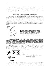
Defect Contribution to the Photoluminescence from Embedded Germanium Nanocrystals Prepared by Ion Implantation and Sputter Deposition Methods P. K. Giri1, Kaustuv Das2, and Samit K. Roy2 1 Department of Physics and Centre for Nanotechnology, Indian Institute of technology Guwahati, Guwahati, 781039, India 2 Department of Physics and Meteorology, Indian Institute of Technology Kharagpur, Kharagpur, 721302, India ABSTRACT In this work, we present a comparative study of vibrational and luminescent properties of Ge nanocrystals (NCs) prepared by ion implantation (Process I) and radio frequency (RF) sputter deposition techniques (Process II). Optical Raman studies reveal presence of strain in the Ge NCs embedded in SiO2 in both cases. Polarization dependent Raman scattering studies show that process I yields NCs with surface symmetrical Raman modes only, whereas process II yields additional surface quadrupolar Raman modes. Photoluminescence studies using 488 nm excitation show broad PL emissions peaked at ~2.3 in all the samples with varying intensities. PL studies on Ar implanted and similarly annealed SiO2 layers confirm that the 2.3 eV emission is originated from oxygen deficient defects in the SiO2 matrix. PL studies with 325 nm excitation show additional strong peaks at higher energies, which are believed to be due to Ge/O interface defects. It is concluded that room temperature visible light emission from embedded Ge NCs is primarily dominated by the oxygen deficient defects in SiOx matrix and non-bridging oxygen surrounding the Ge NCs, while light emission due to quantum confined carriers in the NCs are quenched perhaps due to inherent strain in the embedded NCs. INTRODUCTION Embedded Ge nanocrystals (NCs) have light emitting and charge storage characteristics promising for light emitting devices and nanoscale memory devices, respectively. However, intriguing role of defects and effect of electron and phonon confinements are poorly understood in Ge NCs as compared to their counterpart in Si NCs. Experimental results have rarely met the theoretical predictions regarding the superior optical properties of Ge NCs. Several studies have indicated that the defects in the surrounding matrix are primarily responsible for broad PL in the visible region [1, 2]. Infrared photoluminescence (PL) has also been attributed to defect states in the NCs [3]. Despite the achievement of crystalline Ge NCs prepared by different methods such as ion implantation, sputtering etc, unambiguous evidence for excitonic emission from Ge NCs are lacking in the literature. This is believed to be due to the intriguing role of surface defects and strain in the NCs as well as defects in the embedding matrix. Low frequency Raman scattering has proved to be a powerful tool to monitor surface vibrational modes of embedded NCs [4]. While the optical Raman spectra of Ge NCs of different sizes have been reported, distinctive features of Raman modes dominated by surface atoms and those dominated by interior atoms have not been identified yet.
Data Loading...