Defect free InGaAs-based strain balanced MQW grown on virtual substrate by metallorganic chemical vapor deposition
- PDF / 411,073 Bytes
- 6 Pages / 595 x 842 pts (A4) Page_size
- 2 Downloads / 266 Views
Defect free InGaAs-based strain balanced MQW grown on virtual substrate by metallorganic chemical vapor deposition A. Passaseo, R. Cingolani, M. Mazzer1, M. Lomascolo1, S. Tundo1, L. Lazzarini2, L. Nasi2 G. Salviati2, K.W. Barnham3 National Nanotechnology Laboratory of INFM, Dept. Ing. Innovazione, University of Lecce, via Arnesano Lecce, ITALY 1 CNR-IME Institute, Via Arnesano, I-73100 Lecce, Italy 2 CNR-MASPEC Institute, Parco Area delle Scienze 37/A, I 43010 Fontanini- Parma, Italy 3 Quantum Photovoltaics Group, Imperial College of Science and Technology, London SW7 2AZ, UK
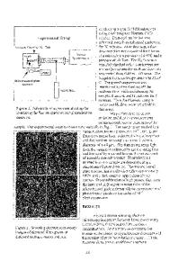
ABSTRACT In this work we describe a novel system for photovoltaic applications which combines InGaAs based strain-balanced multiple quantum wells (MQWs) with a "virtual substrate", designed to extend the absorption edge of the photovoltaic devices to about 1 eV. The virtual substrate is designed by properly choosing a sequence of InGaAs layers having different In content, in order to obtain the desired lattice parameter at the topmost layer and to confine at the deepest interfaces the misfit dislocations, well away from the QW active region. A series of InGaAs p-i-n junctions, containing a strain balanced MQW in the intrinsic region, were deposited by metallorganic chemical vapor deposition on different virtual substrates. In all the samples the virtual substrates were proved to be successful to grow zero net strain MQW and to confine defects at the buffer/substrate interface. Transmission electron microscopy observation shows that no defects propagate from the strain accommodating layers to the active region. The total density of threading dislocations reaching the surface was found to be less than 1*E5/cm2. The confined misfit dislocation network, however, results in marked cross-hatched morphology that was found to affect the lateral strain distribution in the whole structure. By optimizing the growth condition of the structures, the influence of the surface roughness induced by CH pattern is partially suppressed.
INTRODUCTION Strained InGaAs/GaAs quantum wells (QWs) are currently used for a large variety of micro-electronic and optoelectronic devices, including high efficiency photovoltaic cells. However, on such structures, the lattice mismatch places severe limits in extending the absorption edge to significant lower energies and on the number of QWs that can be accommodated before strain relaxation takes place. In order to overcome substrate lattice parameter limitations, strain balanced approach in GaAs based QW solar cell can be used, by compensating the compressive strain of the InGaAs QWs with appropriated tensile strain barriers which lead to an intrinsic region average lattice parameter equal to that of GaAs. With this method a moderate shift in the absorption edge (up to 960 nm), together with an higher density of active layer, have been obtained [1]. However, in order to move the spectral response to significantly higher wavelengths and to obtain a large number of QWs in the intrinsic region without plastic relaxation, is nece
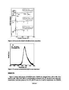
Data Loading...