Defect-Induced Photoluminescence from Pulsed Laser Annealed Si
- PDF / 1,944,190 Bytes
- 7 Pages / 414 x 635.4 pts Page_size
- 100 Downloads / 399 Views
185
DEFECT-INDUCED PHOTOLUMINESCENCE FROM PULSED LASER ANNEALED Si
M S SKOLNICK, A G CULLIS AND H C WEBBER Royal Signals and Radar Establishment, St Andrews Road, Worcestershire, UK.
Great Malvern,
ABSTRACT Low temperature photoluminescence is used to study damage centers in ion implanted, pulsed laser annealed Si. A number of intense, damage related photoluminescence lines W, G and 13 are observed. It is shown that most of the W (and 13) centers are created by solid phase annealing of implant damage beyond the laser melted region. Peak G, on the other hand, is present in the tail of the implant damage before laser annealing.
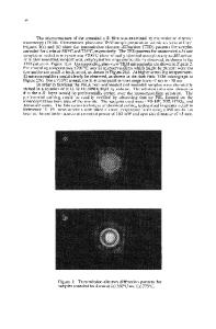
INTRODUCTION Pulsed laser annealing is known to give very good recrystallization of ion implanted Si surfacesI. TEM work has shown that no extended defects remain after such laser annealing2. However, evidence has been published in the last two years using Deep Level Transient Spectroscopy (DLTS) for the presence of relatively high point defect concentrations up to 1016 cm- 3 in laser annealed Si samples . Also the depth of defect annihilation in laser annealed Si has 4 been studied using EBIC techniques . In the present paper, low temperature photoluminescence (PL) is used as a sensitive method for studying point defect centers in ion implanted, pulsed laser annealed Si. Very strong, sharp, luminescence lines together with a broad band arising from various damage centers are observed. Some of the results on two of the sharp line series 5 have been presented in a previous publication . PL studies on CW laser 6 annealed Si have been reported by Street et a1 . They found broad damage related bands as opposed to the sharp line spectra reported below. EXPERIMENTAL AND RESULTS Experiments were carried out on (100) slices of 30ncm n-type Si. Implantations were performed 8 off the (100) direction with 80keV Si ions at doses 2 up to 3 x 1015 cm- . Laser annealing was carried out using single 3Onsec pulses of 6940R radiation from a Q-switched ruby laser. A highly uniform beam profile over a 6mm area was obtained using a silica light guide diffuser7. PL measurements were performed with the samples immersed in liquid He at 4.2K. The luminescence was excited using 150mW of the 488OR line from an unfocused Ar ion laser and detected using a Ge photodiode. Further experimental details are given in Ref 5. A typical PL spectrum for the ion implanted, laser annealed samples is presented in Fig 1. All the luminescence peaks W (1.019eV), G(O.97OeV), 13 (1.039eV) and the broad band X in Fig 1 are damage related and are not present in the starting material. These lines have been observed previously 8 9 in a variety of radiation damage studies , . Lines W, G and 13 are labelled using the notation of Refs 8 and 9. At higher energy lines characteristic of the untreated n-Si including the phosphorus bound exciton line PTO (1.092eV) are observed. (see Ref 5).
186
"20Si, 80 KeV
1+15
• oSc."
-
Fig 1. PL 155lm spectrum at 4.2K
G
5
for 3 x 10 cm-2 implanted sample laser annealed at 1.5J/cm Damage features W,
Data Loading...