Visible Photoluminescence and Microstructure of Annealed and Chemically Etched Amorphous Si
- PDF / 3,186,516 Bytes
- 6 Pages / 420.48 x 639 pts Page_size
- 26 Downloads / 270 Views
VISIBLE PHOTOLUMINESCENCE AND MICROSTRUCTURE OF ANNEALED AND CHEMICALLY ETCHED AMORPHOUS Si
K.H. JUNG*, S. SHIH*, D.L. KWONG*, C.C. CHO**, and B.E. GNADE**
*Microelectronics Research Center, Department of Electrical and Computer Engineering, The University of Texas at Austin, Austin, TX 78712. "**Texas Instruments Inc., P.O. Box 655936, Dallas, TX 75265.
ABSTRACT We have studied the visible photoluminescence (PL) and microstructure of porous Si layers (PSLs) fabricated by the chemical etching of annealed amorphous Si (a-Si). The a-Si layers were partially crystallized by annealing between 5500 C-1 150'C in N2 and the PSL formed by etching in a HF-HNO 3 -based solution. No visible PL was observed after etching of unannealed a-Si. Visible PL was detected after etching a-Si layers first annealed at temperatures ->725*C,coinciding with the observation of Si microcrystallites in the annealed layer prior to etching. The results suggest that an initial crystalline structure is important for fabricating luminescent PSLs.
INTRODUCTION Visible room temperature photoluminescence (PL) from porous Si layers (PSLs) [1] has attracted wide attention recently and generated considerable debate on the origin and mechanism of the PL [2]. Although the exact origin and mechanism are still unclear, the early proposed model centered around quantum-size effects in a Si quantum wire network [1,3] formed in high porosity PSLs. Further research indicates that surface passivation may also play an important role in providing efficient PL [4-5]. Other research suggests that the dominant luminescing material is amorphous in nature [6-7], and may in fact be due to siloxene molecules [8]. PSLs can be fabricated by anodizing bulk Si in an HF-based solution [9-10]. Only recently, however, has the observation of visible PL at room temperature been reported for extremely high porosity PSLs [1]. In practice, numerous variations in anodization cell design are used. In addition, chemical etching in HF-HNO3 -based solutions without applying electrical bias has also been demonstrated to produce luminescent PSLs [6,11].
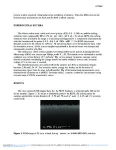
EXPERIMENT AND DISCUSSION In this paper, we report on the changes in the microstructure and the visible PL from PSLs fabricated from amorphous Si (a-Si) films by annealing and chemical etching. The starting substrates were 5-6 n.cm B-doped (100)Si wafers. Amorphous Si layers 2 l.tm thick were grown by3 molecular beam epitaxy at a substrate temperature of 25'C. The films were doped at 1016 cm- with B. A negligible amount of dopant activation is believed to have occurred due to the low growth temperature. No visible PL could be observed from the unannealed a-Si sample under illumination from 365 nm or 254 nm ultraviolet (UV) light. Nor could any visible PL be observed after immersion in HF for several hours. Unprocessed a-Si samples were then annealed in a conventional quartz tube furnace at atmospheric pressure. The samples were annealed in N2 at 550'C-1 150'C for 4 min.
Mat. Res. Soc. Symp. Proc. Vol. 283. ©1993 Materials Research Socie
Data Loading...