Defect Luminescence in Heavily Mg Doped GaN
- PDF / 354,638 Bytes
- 6 Pages / 420.48 x 639 pts Page_size
- 24 Downloads / 385 Views
G 11.8 Mat. Res. Soc. Symp. Proc. Vol. 537 © 1999 Materials Research Society
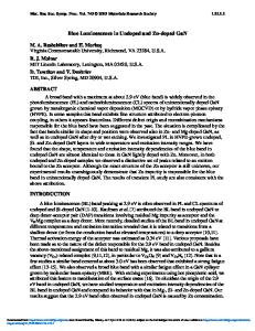
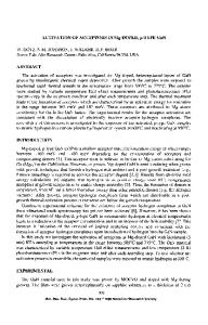
EXPERIMENTAL RESULTS The Mg-doped GaN epilayers were grown on c-plane sapphire by metal-organic vapor phase epitaxy. The samples are either semi-insulating or p-type with resistivity as low as 3 Q.cm at room temperature. PL was excited by cw He-Cd laser (325 nm) and analyzed by Spex grating monochromator with Hamamatsu photomultiplier tube. Excitation power density (Pexc) was varied over the range 10-5 -27 W/cm 2 by means of neutral density filters. The sample temperature was varied from 13 to 380 K using a closed cycle helium cryostat. A broad band with a peak near 2.8 eV has been observed in the PL spectra of the studied samples. In some samples another PL band with a maximum near 3.2 eV was noted as a shoulder or separate peak. The position of the 2.8 eV band depended strongly on excitation intensity (Fig. 1). At low temperature the total blue shift of the band with increasing excitation power amounted to 0.23 eV. The peak position shifted largely at high excitation density and was nearly independent of excitation rate in the low excitation limit. At room temperature the PL band shifted about 0.10 eV over the same excitation intensity range (Fig. 1). The shape of the band remained almost independent of excitation intensity for the samples with small overlap with the 3.2 eV band. A typical change in the PL spectrum is shown in Fig. 2. We attribute the observed dependence of the PL spectrum with excitation to changes in contributions of emission from close and distant pairs in the case of deep DAP transitions. The DAP transition rate for a pair with a separation R has the approximate form 13,14
W(R)=WOexp a
3
II....I~ i 1I... 1. ..1 l . ... q .. .. n GaN:Mg
+ # Y244 (T=13 K) - # Y244 (T=297 K) A #Y247 (T=13 K)
>
2.9 0
0
. ..
•
(I)
.
S En
# Y247 (T=297 K) # Sh64 (T=13 K) K) # Sh64 (T=297
a
++-
C')
+0"
(0
*+
CL 2.8 CZ
CD
• C: tC
X
+A
+
-+
X0L0 A
+ +
.,,-
CL -j
2.7
~iJe I I II.Ii
i -miriJ
5
10-
4
10-
3
10-
I IIIIJ I IIIIJ I In III I III
10-2
10
0.1
102
2
Excitation Density (W/cm ) Fig. 1.Dependence of the 2.8 eV PL peak position on excitation power density at 13 and 297 K for three GaN:Mg samples.
2.4
2.6
2.8
3
3.2
3.4
Photon Energy (eV)
Fig. 2. PL
spectra of the semi-
insulating GaN:Mg sample # Y244 at different excitation intensities.
where aB is the largest Bohr radius for the bound carriers. The radiative lifetime increases exponentially with increasing R according to Eq. (1). At high excitation intensity, PL from distant pairs saturates due to their longer lifetime and transitions between close pairs dominate. The PL energy corresponding to a transition between a pair with separation R is given by EpL(R)
=E
- (EA + ED) •e e
gcR
(2)
where Eg is the band gap, EA and ED are the acceptor and donor binding energies, e is the electronic charge, and c is the low frequency dielectric constant. The last term is due to the Coulomb interaction between charged donor and acceptor. As a
Data Loading...