Defect Structure of the Epitaxial Pd 2 Si-Silicon Interface
- PDF / 745,784 Bytes
- 6 Pages / 417.6 x 639 pts Page_size
- 64 Downloads / 428 Views
Inc.
291
DEFECT STRUCTURE OF THE EPITAXIAL Pd 2 Si-SILICON INTERFACE
D. Cherns(a and D.A. Smith IBM T.J. Watson Research Center, Yorktown Heights, N.Y. 10598
ABSTRACT The crystallography of the epitaxial Pd 2 Si-silicon interface has been analyzed with special reference to the character of interfacial dislocations. It is proposed that the Pd 2 Si which forms at the interface does so by the diffusion stimulated glide of transformation dislocations.
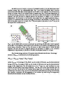
INTRODUCTION Silicon-metal reactions are of great practical importance since they affect the electrical properties of contacts to solid state devices. In addition these reactions have fundamentally interesting kinetic and crystallographic features. In this paper the crystallography and structure of the interface between hexagonal Pd 2 Si and I1111 oriented diamond cubic silicon ar$ analyzed in detail. Previous wprk has established that the interface is epitaxial with (lll)Si // (0001)Pd 2 Si[1] and [112]si// [2110] Pd 2 Si. Transmission electron microscopy has shown that the interface may be stepped locally [2]. The Pd 2 Si is not a single crystal but is composed of domains [3], some but not all of which are thought to be crystallographically equivalent variants of the Pd 2 Si structure. CRYSTAL STRUCTURE The diamond cubic structure of silicon is well known but it is useful to show the atom arrangement projected on (111), fig. Ia, for comparison with the Pd 2 Si structure which is shown in figs. lb and I c. The stacking of the 1111 planes in the diamond cubic structure may be described as ... AaBbCc ..... The stacking of the silicide may be described as .... Aa .... ; the sites designated A,a and a all lie along [1111 and are occupied by silicon atoms except that in the A and a layers of the silicide 1/3 and 2/3 respectively of the silicon sites are vacant, figs. lb and ic. In the A layer of the silicide each vacant Si site is surrounded by an equilateral triangular cluster of Pd atoms at coordinates of the type 0.26,0,0. In the a layer the Pd atoms again form equilateral triangular clusters around the Si vacancies and have coordinates of the type 0.61, 0, 1/2.[4) The lattice parameters are: silicon a = 5.43A and for Pd 2 Si a=6.53A and c=3.44A. The misfit parallel to the [112]and[f1l] directions of the silicon is 0.018 and -0.089 respectively, using silicon as the reference lattice.
INTERFACE STRUCTURE AND TRANSFORMATION OF Si TO Pd 2 Si Formally transformation of Si to Pd 2 Si requires the in-diffusion of 6 Pd atoms and the out diffusion of 3 Si atoms respectively per unit cell of the silicide and the transformation of the cubic .... AaBbCc.... stacking to hexagonal ... Aa... stacking. A possible transformation scheme is shown in fig. 2. Transformation dislocations with Burgers vectors of the form 6 + A[111] SV/
6
6
/ is the change in spacing of the (Ill) planes indicated in 6 fig. 2, are postulated to glide in response to the chemical stress resulting from the fluxes of Pd and Si. i.e. 1, where 6
ýa Permanent Address: Oxford, England.
Oxford University, Dept
Data Loading...