Deposition of Functionalised Gold Nanoparticles by the Layer-by-Layer Electrostatic Technique
- PDF / 566,003 Bytes
- 6 Pages / 612 x 792 pts (letter) Page_size
- 57 Downloads / 363 Views
N9.12.1
Deposition of Functionalised Gold Nanoparticles by the Layer-by-Layer Electrostatic Technique S. Paula,*, M. Palumbo,a M. C. Petty,a N. Cantb and S. D. Evansb a
School of Engineering and Centre for Molecular and Nanoscale Electronics, University of Durham, Durham DH1 3LE, UK b Department of Physics and Astronomy, University of Leeds, Leeds LS2 9JT, UK
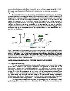
ABSTRACT Intensive research is currently underway to exploit the intriguing optical and electronic behaviour of nano-sized particles. The basis of the unique properties of these particles is the smallness of their size; dimensions on the nanometre scale can result in interesting quantum mechanical phenomena, such as Coulomb blockade. There are currently a number of ways by which the nanoparticles can be deposited onto solid substrates. Here, we report on the use of the layer-by-layer electrostatic method, which has shown much promise in the context of deposition of thin films of certain organic materials. In this technique, layers of oppositely charged materials are generated by dipping an appropriate substrate into solutions of polyelectrolytes. For example, the polybases poly(ethyleneimine) (PEI), when adsorbed on a substrate, produce a positively charged surface. We have deposited carboxylic acid (-COOH) derivatised gold nanoparticles onto a PEI-coated silicon substrate and an amine funtionalised silicon substrate. The distribution of the gold nanoparticles was compared using atomic force microscopy.
INTRODUCTION Nanoparticulate materials of semiconductors [1, 2] and metals [3, 4] are currently the focus of intense research. The physical properties of such small-scale structures can be tailored for particular applications. For example, their electronic and chemical behaviour can be changed simply by controlling the particle size. Nanoparticles also provide useful building blocks from which complex molecular architectures can be built. In the field of microelectronics, the 1-20 nm scale length that is typically associated with nanoparticles paves the way for achieving high device densities. Quantum mechanical effects, such as Coulomb blockade, may also be exploited in device structures such as the single electron transistor [5]. We have recently demonstrated the use of gold nano-particles in the fabrication of memory devices [2]. The encouraging aspect of this work was that the deposition of the gold nanoparticles was carried out at room temperature, both by the Langmuir-Blodgett as well as via chemical routes. Attempts have been made in the past to utilise nano-crystallites of silicon to build memory devices (Tiwari et. al [6 ]). However, the nanoparticle deposition was carried out at high temperatures. *
Present address: Department of Ceramic and Materials Engineering, The State University of New Jersey 607 Taylor Road, Piscataway, NJ 08854-8065, USA
N9.12.2
An alternative to silicon-based technologies (which generally requires operation at high temperatures) is to use organic materials. The devices generated from such materials can be inexpensive,
Data Loading...