Depth-Resolved Microspectroscopy of Porous Silicon Multilayers
- PDF / 817,671 Bytes
- 6 Pages / 417.6 x 639 pts Page_size
- 53 Downloads / 400 Views
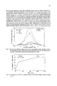
ABSTRACT We have measured micro-photoluminescence (PL) and micro-Raman spectra on the cross section of porous silicon multilayers to sample different layer depths. We find noticeable differences in the spectra of layers with different porosity, as expected from the quantum confinement of electrons and phonons in silicon nanocrystals with different average sizes. The PL emission band gets stronger, blue shifts, and narrows at the high porosity layers. The average size can be estimated from the shift. The Raman phonon band at 520 cm-1 weakens and broadens asymmetrically towards the low energy side. The line shape can be related quantitatively with the average size by the phonon confinement model. To get a good agreement with the model we add a band at around 480 cm- 1 , which has been attributed to amorphous silicon. We also have to leave as free parameters the bulk silicon phonon frequency and its line width, which depend on temperature and stress. We reduced laser power to eliminate heating effects. Then we use the change of frequency with depth to monitor the stress. At the interface with the substrate we find a compressive stress in excess of 10 kbar, which agrees with the reported lattice mismatch. Finally, average sizes are larger than those estimated from PL.
INTRODUCTION Porous silicon, obtained by electrochemical etching of doped silicon, consists of a silicon skeleton with nanometer-size crystallites. The discovery of visible light emission at room temperature in porous silicon [1] has raised expectations for the application of silicon in optoelectronics devices, like light-emitting diodes. Moreover, the refractive index of porous silicon depends strongly on porosity. By changing the etching current during sample preparation, the index can be varied continuously between the indices of bulk silicon and air. As the etching takes place mainly at the deepest layer, without affecting previously etched layers, the porosity can be varied freely with depth. This opens the way for complex photonic devices based entirely on silicon. For example, porous silicon multilayers [2], where the porosity varies periodically with depth, have been used in filters [2], dielectric mirrors [3], waveguides [4], and optical microcavities [5]. In these structures it is very important to study the variation of their properties with depth. Microspectroscopic measurements on a cross-section, which have been reported for porous silicon single layers [6, 7], can determine the optical properties and the size of silicon nanocrystals with a spatial resolution of I pm. In multilayers reports have limited to top and bottom surface measurements [8]. The only cross-sectional studies correspond to X-ray diffraction [9].
155 Mat. Res. Soc. Symp. Proc. Vol. 588 © 2000 Materials Research Society
ubstat
10 utm
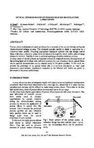
Figure 1: The cross section for a 61%/86% porous silicon multilayer as seen with the optical microscope. High porosity layers appear as dark bands. They show strong emission at 1.8 eV in the photoluminescence image (inset). In this work w
Data Loading...