Determination of Surface Space Charge Density on Semiconductor from Displacement Current-Voltage Curve using a Scanning
- PDF / 137,695 Bytes
- 6 Pages / 612 x 792 pts (letter) Page_size
- 99 Downloads / 353 Views
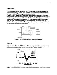
Determination of Surface Space Charge Density on Semiconductor from Displacement Current-Voltage Curve using a Scanning Vibrating Probe Yutaka Majima, Tomohiko Masuda, Setsuri Uehara, Atsushi Okuda, and Mitsumasa Iwamoto Department of Physical Electronics, Tokyo Institute of Technology 2-12-1 O-okayama, Meguro-ku, Tokyo 152-8552, JAPAN ABSTRACT A determination method of the local surface space charge density in thin films on semiconductor surfaces is described. In this method, the displacement current and the tunneling current flow periodically in accordance with the perpendicular vibration of the probe of the scanning tunneling microscopy (STM). The external circuit current is separated into the mean displacement current and the mean tunneling current by using the two-phase lock-in amplifier. The displacement current-probe voltage curve of a p-type silicon with a native oxide layer was measured in a vacuum (< 3x10⁻⁹ torr). The displacement current-voltage curve has been analyzed taking into account surface space charge. The theoretical displacement current-voltage curve has been fitted to the measurement in order to obtain both the local surface space charge density and the surface potential difference of thin films, and the theory is in good agreement with the measurement in both voltage regions where the majority carriers are accumulated and depleted. We also demonstrate a simple determination method of both the surface space charge density and the surface potential difference of thin films from flat-band conditions in the displacement current-voltage curve. INTRODUCTION The electronic properties of surface space-charge densities on semiconductors have been investigated for a number of years, since it is directly related to most planar device properties [1]. Capacitance-voltage (C-V) measurement on the metal-insulator-semiconductor structure has been used, and charges in the insulator have been evaluated from flat-band voltage shift in the C-V dependence. Recently the scanning probe microscopy (SPM) such as scanning tunneling microscope (STM), atomic force microscope (AFM) and scanning capacitance microscope (SCaM) has attracted considerable interest from the viewpoint of semiconductor surface physics [2,3]. STM is able to be used to obtain local spectroscopic information about the electronic structure of surfaces. STM and AFM have been widely used for observation of surface image with nanometer-scale lateral resolution. In SCaM, an oscillation voltage is applied to the probe, and the change in the capacitance between the probe and the sample is detected by a change in the resonant frequency using a UHF resonant capacitance sensor. The local charge trapping in SiO2/Si system have been reported by using a combined SPM including AFM and SCaM [4]. It is significant to investigate the relationship between electronic structure and local carrier concentration of semiconductors. Recently we have developed a simultaneous measuring system of tunneling current and displacement current using a scanning vibrating probe [5-8]
Data Loading...