Imaging of Cracks in Semiconductor Surfaces Using Scanning Tunneling Microscopy
- PDF / 2,171,087 Bytes
- 6 Pages / 420.48 x 639 pts Page_size
- 16 Downloads / 403 Views
IMAGING OF CRACKS IN SEMICONDUCTOR SURFACES USING SCANNING TUNNELING MICROSCOPY
T. FOECKE*, R. KING**, A. DALE* and W.W. GERBERICH* *Dept of Chemical Engineering and Materials Science, University of Minnesota, Minneapolis, MN 55455 "**OpticalRecording Division, 3M Company, Vadnais Heights, MN 55110
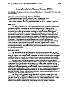
ABSTRACT Scanning Tunneling Microscopy (STM) has developed into a useful tool for atomic-scale characterization of material surfaces. It is proving especially useful in the field of fracture, as the vast majority of high-resolution images of fracture processes are made in the transmission electron microscope, where thin film effects and sample preparation may greatly modify crack tip stresses and dislocation structures. This investigation involved imaging of cracks introduced in Si at room temperature and single crystals of galena (PbS) by rapid indentation at 77K. Images were obtained at the arrested crack tip, around the indentation, and along the flanks of the crack in the dynamic growth region. Measurements were made of both crack-tip morphology and upsets observed along the flanks of the cracks in PbS. Interesting results concerning crack tip geometry in Si, the effect of STM tip geometry and scan conditions on the resulting image of the cleavage crack, as well as work in progress on other material systems, will be discussed.
INTRODUCTION The STM has been used in the past to obtain high-resolution images of incidental surface cracks [1], indentations [2,3], manufactured structures [4,51, and surface damage [6,7]. The first reported images of induced cracks in semiconductors were presented by Bonnell and Clarke [8]. These studies have shown that STM can be very useful in obtaining quantitative topographical information about surface defect structures. To be able to understand the fundamental physical mechanisms that control brittle crack stability in materials, it is necessary to know the atomic structure and atom displacements at the tip of a brittle crack. High resolution imaging of cracks has always been performed in the transmission electron microscope [9,10], where sample thinning may change the dislocation structure and associated stress state. Also, some of these studies examine cracks formed by tearing upon loading an electropolished hole [9]. In this case, the loading mode and history cannot be accurately determined, and independent quantitative data is not possible. With the advent of scanning tunneling and scanning force microscopies, it has become possible to obtain atomic resolution images of semiconducting and conductive surfaces directly without extensive sample preparation. These techniques thus could provide a real, high resolution image of the threedimensional displacement field at the tip of a crack with a well-characterized loading history, such as those introduced by indentation fracture.
Mat. Res. Soc. Symp. Proc. Vol. 209. Q1991 Materials Research Society
618
EXPERIMENTAL PbS was obtained as polycrystalline aggregates of the natural mineral galena with crystallites on the order of centim
Data Loading...