Determination of the Mechanical Properties of Polysilicon Thin Films Using Bulge Testing
- PDF / 1,462,944 Bytes
- 6 Pages / 414.72 x 648 pts Page_size
- 9 Downloads / 353 Views
directions forming near perfect orthogonal windows. An exact solution for the deflection of square membranes under an applied pressure has been derived [3], but is too cumbersome to be suitable for the analysis of bulge test data. Approximate solutions [4-7] using the energy minimization method relate the deflection of the center of,the square membrane (hmax) to the applied pressure (P) and the residual stress in the film (ao) as:
P= C1 (v)
Et
+
4
ha +C2
2t __
h hmax
(1)
where t is the thickness of the film, 2a is the dimension along the side of the square window, E is the elastic modulus of the film, v is the Poisson's ratio of the film, C,(v) is constant for a given material and depends only on Poisson's ratio and C2 is a dimensionless constant that is independent of the material properties and has a value of 3.393 for square membranes. Vlassak and Nix [6] have shown that C,(v) for square membranes can be approximated as: Csquare(v) =
I
V3(2)
(0.792 + 0.085v) 3
This approximation has been used in the current study because the predicted variation of C,(v) has been shown to agree very well with finite element calculations [7]. The form of the exact solution for rectangular membranes with large aspect ratios is identical to equation (1), except C1 (v) is given by: 623 Mat. Res. Soc. Symp. Proc. Vol. 505 ©1998 Materials Research Society
Crectangie(V) =
8
(3)
60l+ W
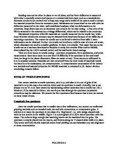
and C2 has a value 2.0. These bulge test equations suggest that plotting the bulge test data as P/hmax verses hmax 2, would give a straight line for both square and rectangular windows, the intercept of which would enable the determination of the residual stress in the film and the slopes from the square and the rectangular samples would yield values for the elastic constants E and v. EXPERIMENTAL PROCEDURES The polysilicon samples for the present study were deposited on (100) oriented n-type Si substrates at the Microelectronics Center of North Carolina (MCNC) in the multi-user MUMPS-12 run and are identical to the samples used in the microsample tensile tests by Sharpe et. al [8]. Three inch diameter wafers were processed by MCNC and then sliced into individual dye sights. The as-received specimens were 1 cm x 1 cm square chips of the silicon substrate covered with: a 600 nm layer of SixN a 2 gtm layer of Phosphosilicate glass (PSG), 2 Pam layer of polysilicon (Poly-1) followed a 1.5 m layer of polysilicon (Poly-2). The details of the deposition process are given elsewhere [9]. The square and rectangular windows were subsequently etched into the silicon substrates at the Applied Physics Laboratory of the Johns Hopkins University. The etching process is described in detail, elsewhere [9]. Fig. 1 shows a typical optical macrograph of an etched sample containing both a square membrane and a rectangular membrane on the same chip.
1 cm
1.2
1 cm Fig. 1: Macrograph of the windows in an etched polysilicon sample.
The bulge tester set-up is schematically shown in fig. 2 and comprises: (i) the pressure application system, (ii) a pressure sens
Data Loading...