Development of Field Emission Flat Panel Displays at Motorola
- PDF / 1,545,523 Bytes
- 3 Pages / 414.72 x 648 pts Page_size
- 75 Downloads / 299 Views
Fig. 1. A 14 cm diagonal, full color FED, with 1/4 VGA resolution and a brightness of 300 Cd/mA2 made at Motorola FPDD. The thinness and flatness of a FED are achieved by replacing the single thermionic cathode of the CRT with a matrix-addressed array of cold electron emission sources. Every pixel in a FED has its own set of cathodes, which are made up of hundreds of sharp, pyramid-shaped metal microtips, as shown in the figure below. The high electric field required for field emission (-1V/A) is achieved by making the tips very sharp (typical radius of curvature of the tips is less than 100nm) and by surrounding each tip with a gate electrode only -0.5 pM away. A schematic structure of a microtip based FED is shown in Fig. 2. A scanning electron micrograph of an actual microtip array made at Motorola is shown in Fig. 3.
21 Mat. Res. Soc. Symp. Proc. Vol. 509 0 1998 Materials Research Society
Gatel (Row) Dielectric
l
11p
Column ! One Electron Emitter Tip
Phoshors
Screen
s Drlver•Cs
Row(CVla N
One Pixel
mi Package
Row IColumns, Emitters
Assembled Display
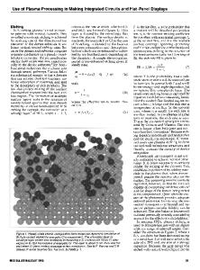
Fig. 2 A schematic structure of a FED based on a Spindt-type cathode.
Fig. 3 A scanning electron micrograph of a microtip array made at Motorola FPDD (top), and a cross-section SEM of one of the tips (bottom). 22
Motorola is currently addressing a number of key development and manufacturing challenges in order to introduce FEDs to the original equipment manufacturer (OEM) and consumer marketplace. For example, the microtips must be highly uniform in shape to produce consistent emission across the entire panel because the emission current depends exponentially on the sharpness of the emitter. This high uniformity can only be achieved by evaporating the tip material at a very large distance between the panel and the metal evaporator. As with any new technology, cost and durability are also issues that must be addressed. Motorola is responding in a number of ways, including increasing the gate hole dimensions which allows for easier, less expensive, manufacturing processes, and by both improving the vacuum inside the panel and making the emitter tips more robust, which increases the lifetime of the FED. Motorola is also concentrating on a number of factors that will provide substantially better viewability over current flat panel technologies. For example, by increasing the brightness and the color gamut of the phosphors, FEDs will offer crisper, clearer and more attractive screen images. Confident that FEDs will be a winning display solution in the marketplace, Motorola is already working on the next iteration of the technology, which will be based on a whole new class of field emission materials, such as carbon. These will be less expensive to manufacture, will deliver higher currents at lower voltages, will require a less strict vacuum in the panel, and will be compatible with a wider range of phosphors.
23
Data Loading...