Development of In-Situ Surface Observation System with an Atomic Resolution under Tensile Stress by Atomic Force Microsc
- PDF / 448,226 Bytes
- 6 Pages / 612 x 792 pts (letter) Page_size
- 11 Downloads / 350 Views
Y8.5.1
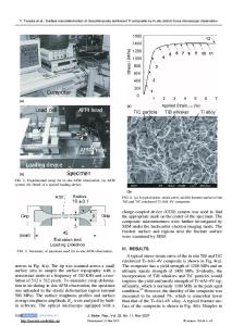
Development of In-Situ Surface Observation System with an Atomic Resolution under Tensile Stress by Atomic Force Microscope Akihito Matsumuro, Kimiharu Kayukawa, Youhei Fujimoto, Taeko Ando and Kazuo Sato Department of Micro System Engineering, Nagoya University, Chikusa-ku, Nagoya 464-8603, Japan ABSTRACT A new in-situ surface observation system under tensile stress with an atomic resolution has been developed for the purpose of the explanation of the deformation of the surface and the crack growth mechanism for thin films in the micro- and nano-mechanical systems. The mechanical properties such as Young’s modulus can be determined at the same time. This observation system consists of the on-chip tensile testing system and a commercialized atomic force microscope (AFM). The on-chip testing system is characterized by a static loading mechanism with a flat spring and a test chip of single-crystal silicon of 15×15×0.5 mm. Particular attention has been paid to the suppression of the vibration which effects on images of the surface with an atomic resolution. Atomic images of the surface of mica can be observed under various tensile strains till the occurrence of the fracture. The growth of the cracks and Young’s modulus for TiN thin film deposited on silicon (100) specimen can be also clarified.
INTRODUCTION Numerous microelectromechanical system (MEMS) devices have been developed, and furthermore nano-technology has been focused on in recent years. In these scientific fields, the mechanical properties of thin films and the surface morphologies with an atomic resolution play an important role in their functions. Many studies of the surface morphologies at the static state without applied stresses have been reported. In order to improve the micro- and nano-technologies for engineering applications, we should understand the change of the surface morphologies under tensile stress and the intrinsic mechanical properties such as the origin of the crack propagation mechanism. For these purposes, the development of an in-situ surface observation system with an atomic resolution under various tensile stress using the atomic force microscopy (AFM) must be a powerful method. Some attempts of micro-scale in-situ tensile studies using AFM, scanning tunneling microscopy (STM) and scanning electron microscopy (SEM) have been reported [1-2]. For a better understanding of nano- and atomic-structures, an in-situ surface observation system with an atomic resolution at ambient stresses and strains should be developed. However, no system with an atomic resolution under continuous variable stress has been developed due to the difficulty of overcoming the vibration, which affect on atomic scale AFM images in the case of applying the tensile stress to the samples. K. Sato et al. [3] have developed the ‘on-chip testing method’ for evaluating mechanical properties of thin film materials. This method enables a uni-axial tensile testing of thin film materials to be carried out directly on the silicon chip with a lever structure in the me
Data Loading...