Device processing and junction formation needs for ultra-high power Ga 2 O 3 electronics
- PDF / 2,789,967 Bytes
- 11 Pages / 612 x 792 pts (letter) Page_size
- 67 Downloads / 273 Views
rospective Article
Device processing and junction formation needs for ultra-high power Ga2O3 electronics Fan Ren, J.C. Yang, and Chaker Fares, Department of Chemical Engineering, University of Florida, Gainesville FL 32611, USA S.J. Pearton, Department of Materials Science and Engineering, University of Florida, Gainesville FL 32611, USA Address all correspondence to S.J. Pearton at [email protected]fl.edu (Received 16 November 2018; accepted 2 January 2019)
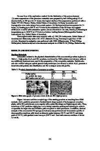
Abstract A review is given of the future device processing needs for Ga2O3 power electronics. The two main devices employed in power converters and wireless charging systems will be vertical rectifiers and metal oxide semiconductor field effect transistors (MOSFETs). The rectifiers involve thick epitaxial layers on conducting substrates and require stable Schottky contacts, edge termination methods to reduce electric field crowding, dry etch patterning in the case of trench structures, and low resistance Ohmic contacts in which ion implantation or low bandgap interfacial oxides are used to minimize the specific contact resistance. The MOSFETs also require spatially localized doping enhancement for low source/drain contact resistance, stable gate insulators with acceptable band offsets relative to the Ga2O3 to ensure adequate carrier confinement, and enhancement mode capability. Attempts are being made to mitigate the absence of p-type doping capability for Ga2O3 by developing p-type oxide heterojunctions with n-type Ga2O3. Success in this area would lead to minority carrier devices with better on-state performance and a much-improved range of functionality, such as p-i-n diodes, Insulated Gate Bipolar Transistors, and thyristors.
Introduction Wide-Bandgap (WBG) semiconductor devices are promising candidates for next-generation power electronic converters.[1–9] Power electronic applications range from on-chip power converters to very high voltage rectifiers for electric power transmission lines.[2,3,7–9] The potential application space includes power generation (solar and wind), power distribution and conversion in electricity grids, electric vehicles, server farms, and charging infrastructure.[2,7–9] High-voltage switching transistors used in these applications are required to have small ON resistance while providing very high blocking voltages in the OFF state. There are already kV-range power switches today, based on SiC and GaN.[7–9] These include a 1200 V directdriven SiC Junction Field Effect Transistor power switch[8] and reliable GaN Metal Oxide–Semiconductor (MOS) Heterostructure Field Effect Transistors (HFETs).[9] The β-polymorph of Ga2O3 has an even larger power figure-of-merit than these two materials and is available in large area bulk and epitaxial layer form.[1–3,6] The potential target for the Ga2O3 devices, if the material quality continues to improve and appropriate device processing techniques are developed, will be in the 100s of kV–MV range.[2] However, the prohibitive cost and limited variety of device types currently possible are still the main constra
Data Loading...