Dielectric GlueWafer Bonding For 3D ICs
- PDF / 513,953 Bytes
- 6 Pages / 612 x 792 pts (letter) Page_size
- 40 Downloads / 340 Views
E5.8.1
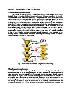
Dielectric Glue Wafer Bonding For 3D ICs Y. Kwon, A. Jindal, J.J. McMahon, J.-Q. Lu, R.J. Gutmann, and T.S. Cale Focus Center - New York, Rensselaer: Interconnections for Gigascale Integration Rensselaer Polytechnic Institute, Troy, New York 12180-3590 ABSTRACT A process to bond 200 mm wafers for wafer-level three-dimensional integrated circuit (3D-IC) applications is discussed. Four-point bending is used to quantify the bonding strength and identify the weak interface. Using benzocylcobutene (BCB) glue, the bonding strength depends on (1) glue thickness, (2) glue film preparation, and (3) materials and structures on the wafer(s). A seamless BCB-to-BCB bond interface provides the highest bonding strength compared to other interfaces in these structures (> 34 J/m2). Mechanical and electrical properties of a wafer with copper interconnect structures are preserved after wafer bonding and wafer thinning, confirming the potential of the bonding process for 3D ICs. INTRODUCTION Wafer level vertical or three-dimensional (3D) integration is one emerging technology being pursued to increase interconnect performance and functionality of ICs [1-3]. Figure 1 shows a schematic of the test vehicle for our 3D integration approach, where fully processed wafers (with multilevel on-chip interconnects) are aligned and bonded with dielectric glue, followed by top-wafer thinning and inter-wafer interconnection using high aspect ratio vias [2]. We have developed a baseline wafer bonding process, a critical process in our approach to wafer level 3D integration, using dielectric polymers [2, 4]. In this work, we use a four-point bending technique to measure the bonding strength and identify the weak interface in various wafer stacks. Systematic bonding experiments using benzocylcobutene (BCB) as the bonding glue are discussed in this paper; we vary (1) glue layer thickness, (2) glue film preparation, and (3) materials and structures on the wafer surface. Since wafer bonding Bridge Via Plug Via might well be used to bond wafers Dielectric that have been processed through 3rd Level Substrate Device multilevel metallization, it needs to (Thinned surface be compatible with essentially Substrate) Bond semiconductor back-end IC Dielectric (Face-to-back) processing steps. As a start to 2nd Level Substrate Device evaluating such compatibility, the (Thinned surface Substrate) impacts of wafer bonding on Bond mechanical and electrical properties (Face-to-face) of a wafer with a two-level back-end Multi-level on-chip interconnects 1st Level Device copper interconnect structures surface Substrate (provided by International Figure 1. 3D integration scheme using wafer SEMATECH) is also evaluated. bonding and inter-wafer interconnection.
Downloaded from https://www.cambridge.org/core. La Trobe University, on 21 Jul 2019 at 06:30:27, subject to the Cambridge Core terms of use, available at https://www.cambridge.org/core/terms. https://doi.org/10.1557/PROC-766-E5.8
E5.8.2
FOUR POINT BENDING TECHNIQUE
Load (N)
This technique was developed to P
Data Loading...