Direct Growth of III-V Devices on Silicon
- PDF / 768,064 Bytes
- 6 Pages / 612 x 792 pts (letter) Page_size
- 16 Downloads / 230 Views
1068-C02-01
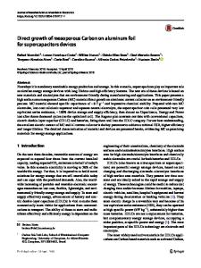
Direct Growth of III-V Devices on Silicon Katherine Herrick1, Thomas Kazior2, Amy Liu3, Dmitri I. Loubychev3, Joel M. Fastenau3, Miguel Urteaga4, Eugene A. Fitzgerald5, Mayank T. Bulsara5, David Clark6, Berinder Brar4, Wonill Ha4, Joshua Bergman4, Nicolas Daval7, and Jeffrey LaRoche2 1 Advanced Technology, Raytheon Tewksbury, Tewksbury, MA, 01876 2 Advanced Technology, Raytheon RF Components, Andover, MA, 01810 3 IQE Inc., Bethlehem, PA, 08873 4 Teledyne Scientific Company, Thousand Oaks, CA, 91360 5 Department of Materials Science and Engineering, Massachusetts Institute of Technology, Cambridge, MA, 02139 6 Raytheon Systems Limited, Glenrothes, Scotland, United Kingdom 7 SOITEC, Bernin, France ABSTRACT Our direct growth approach of integrating compound semiconductors (CS) and silicon CMOS is based on a unique silicon template wafer with an embedded CS template layer of Germanium (Ge). It enables selective placement of CS devices in arbitrary locations on a Silicon CMOS wafer for simple, high yield, monolithic integration and optimal circuit performance. HBTs demonstrate a peak current gain cutoff frequency ft of 170GHz at a nominal collector current density of 2mA/μm2. To the best of our knowledge this represents the first demonstration of an InP-based HBT fabricated on a silicon wafer. INTRODUCTION Combining the best attributes of Compound Semiconductors (CS) and CMOS (complementary metal–oxide–semiconductor) will enable performance superior to that achievable with CS or CMOS alone with CMOS affordability. With an approach that directly integrates the CS into the CMOS wafer, only one wafer is processed to achieve a finished chip. In contrast, device transfer and wafer bonding approaches require fabrication of separate CMOS and CS wafers, followed by assembly. The starting material, shown in Figure 1, is based on a unique silicon template wafer invented at MIT and fabricated by Soitec [1,2,3]. These silicon-on-lattice-engineered substrates (SOLES) contain an embedded CS template layer of Germanium (Ge). This unique wafer technology enables placement of CS devices in arbitrary locations on the chip, while maintaining co-planarity with the CMOS for simple, high yield, monolithic integration. Si SiO2 CS template (Ge interface) SiO2 Si substrate
Figure 1. Soitec’s Silicon on Lattice Engineered Subtrates (SOLES)
A cross section of CMOS and InP HBT integration on SOLES is shown in Figure 2. The process flow on the SOLES template wafer is as follows 1) front end CMOS device fabrication, 2) selective window opening for the HBT devices, 3) InP HBT epitaxial growth, 4) InP HBT device processing, and 5) interconnects between the InP HBT devices and CMOS. nmos
InP HBT
pmos
CS template (Ge interface) Si substrate
Figure 2. Cross-section of CMOS and InP HBT Integration on SOLES EPITAXIAL GROWTH ON GEOI SUBSTRATES The initial process development of InP HBT epitaxy and devices on silicon is with GeOI (Germanium on Insulator) silicon substrates shown in Figure 3. This allows for the development of epitaxial gro
Data Loading...