Dislocation density reduction in heteroepitaxial III-V compound films on Si substrates for optical devices
- PDF / 783,724 Bytes
- 9 Pages / 594 x 792 pts Page_size
- 104 Downloads / 403 Views
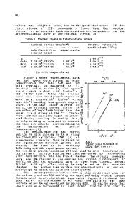
The reduction of dislocation density in heteroepitaxial III-V compound films on Si substrates has been studied using MOCVD (Metal-Organic Chemical Vapor Deposition). High-quality GaAs films on Si, with a dislocation density of about 106 cm"2, have been obtained by combining strained-layer superlattice insertion and thermal cycle annealing. Reduction of dislocation density in the III-V compounds on Si is discussed based on a simple model, where dislocation annihilation is assumed to be caused by dislocation movement under thermal and misfit stress. As a result of dislocation density reduction, high-efficiency GaAs-on-Si solar cells with total-area efficiencies of 18.3% (AMO) and 20% (AM1.5), and red and yellow emissions from InGaP-on-Si light-emitting diodes have been realized. Moreover, future prospects of heteroepitaxy of III-V compounds on Si are also discussed.
I. INTRODUCTION Heteroepitaxy of III-V compounds on Si substrates is receiving strong interest1 because heterostructures of III-V/Si are promising for monolithic integration of III-V devices, Si devices, and opto-electronic integrated circuits. This heteroepitaxial technology will also provide low-cost, lightweight, and large-area III-V compound substrates with high mechanical strength and excellent thermal conductivity. There are, however, three major problems in obtaining high quality III-V films on Si. One is anti-phase domain generation due to the polar-on-nonpolar system. The second is high density dislocation generation due to large differences of lattice constants and thermal expansion coefficients between III-V compounds and Si. The last is residual stress due to the large difference in their thermal expansion coefficients. In order to obtain high-performance III-V devices on Si, it is especially important to reduce the density of dislocations, which act as recombination centers and reduce minoritycarrier lifetimes. This paper describes the reduction of dislocation density in heteroepitaxial III-V compound films on Si substrates and the application of heteroepitaxy on Si to solar cells and light-emitting diodes (LEDs). Mechanisms of dislocation density reduction in III-V/Si by thermal cycle annealing and strained-layer superlattice insertion are discussed. Moreover, the possibilities of the application of this technology to several optical and electron devices are also reported. II. HETEROEPITAXIAL GROWTH OF III-V/Si
GaAs, GaP, InP, and InGaP films were directly grown on Si substrates using low-pressure MOCVD sys376 http://journals.cambridge.org
J. Mater. Res., Vol. 6, No. 2, Feb 1991 Downloaded: 21 Mar 2015
tems. The substrates were Si(100) 2-4° tilted toward [Oil]. Trimethyl-gallium (TMG) or triethylgallium (TEG) as a gallium source and trimethylindium (TMI) as an indium source were used. As3 and PH3 were used as As and P sources. The growth sequence2 is as follows. Si substrates were degreased and etched just before loading into the reactor. To remove native oxide from the Si surface, the substrates were preheated at about 1000 °C in an H 2
Data Loading...