Heteroepitaxy of InP on Si for Optical Devices
- PDF / 1,958,387 Bytes
- 9 Pages / 420.48 x 639 pts Page_size
- 50 Downloads / 405 Views
HETEROEPITAXY OF InP ON Si FOR OPTICAL DEVICES Hidefumi Mori, Mitsuru Sugo, and Masafumi Yamaguchi*
Masami Tachikawa,
NTT Opto-electronics Laboratories, 3-1 Morinosato 243-01. *Tokai, Ibaraki-ken 319-11, Japan
Yoshio Itch, Atsugi,
Kanagawa
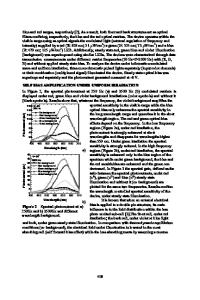
ABSTRACT In situ measurements of dislocations at growth temperature have been made on the heteroepitaxial systems of GaAs/Si and GaP/Si. It was found that the etch pit densities of heteroepitaxial layers were as low as those of bulk wafers at the growth temperature and increase to 107 cmwhen the layers cool down to room temperature. This means that the thermal stress determines the quality of heteroepitaxial layers. The InP on Si system, in which the thermal expansion coefficient difference is smaller than other heteroepitaxial systems, has been studied. High quality InP has been obtained using a GaAs buffer layer, strained-layer superlattice insertion, and thermal cycle annealing and regrowth. Full width at half maximum of X-ray rocking curve was 110" at 13 •m thickness. An InGaAsP laser diode emitting at 1.55 um was successfully made on Si. The threshold current was 46 mA at room temperature for a ridge waveguide laser with a 4 um width and a 200 ,um cavity length. i.
INTRODUCTION
Heteroepitaxy of III-V compounds on Si is attracting interest for its application to opto-electronic integrated circuits(OEICs). However, the high dislocation density in the heteroepitaxial layer is the major problem in making various devices on Si, especially optical devices such as laser diodes(LDs) and detectors. The cause of the dislocations in growth process, lattice or thermal mismatch must be clarified. InP and related compounds crystals have attractive features such as applications to long-wavelength optical devices and a lower degradation by dislocations than GaAs-based devices.[l] InP heteroepitaxy on Si may be suitable for integration of InP optical devices and Si electronic devices. A 1.3 Mm laser on Si has been made recently, [2] however, there are no reports of 1.55 Sm laser diodes which are important devices in optical communication. This paper reviews our recent research on in situ etching of the heteroepitaxial layer to clarify the origin of high dislocation density. High quality InP growth on Si and its application to long-wavelength (1.55 #m) laser diode fabrication are discussed. 2.
IN SITU ETCHING OF HETEROEPITAXIAL
LAYER
High tensile residual stresses have been observed in III-V layers on Si, as listed in Table I. Thermal stresses calculated from a bimetal model are approximately 10p dyn/cm . Experimental Mat. Res. Soc. Symp. Proc. Vol. 198. §1990 Materials Research Society
120
values are slightly lower, but in the predicted order. If the yield stress of III-V compounds is lower than the residual stress, it is possible that dislocations are introduced in the heteroepitaxial layer by the residual stress.[3] Table I
Thermal stress in heteroepitaxial layers
Thermal stress(dyn/cm2 ) calculated from bimetal model
Thermal expansign coefficient(°C-)
experimental 6
Si G
Data Loading...