Dislocation Mechanisms of Relaxation in Strained Epitaxial Films
- PDF / 2,370,800 Bytes
- 9 Pages / 576 x 777.6 pts Page_size
- 81 Downloads / 388 Views
52
in cases involving conduction normal to the interface or other special situations. However, in recent years, the control objective has shifted for some applications. In many planar devices with lateral transport, dislocations at an interface are not necessarily deleterious, so the goal has been modified to eliminate threading dislocations, which extend across the thickness of a thin film. Such dislocations can act as paths of relatively easy charge transport, as diffusion paths for dopants or as surface seeds for defects in subsequent overgrowth or processing steps. Even though the resulting interface may be significantly dislocated, strained-layer epitaxy provides the means to fabricate films of difficult-to-grow materials with low defect density in the electronically active regions. Chances of complete coherency across an interface are best for lattice-matched systems, which have materials with the same crystal structure and nearly identical lattice parameters. However, as observed early in the pursuit of useful heterostructures, a small mismatch of lattice parameter between a substrate and a film being deposited on it could be accommodated by elastic strain of the film as it grows. Furthermore, elastic strain directly influences the electronic band structure of a semiconductor material. This adds an important dimension to the design of heterostructures when electronic properties can be influenced by mechanical strain in a thin film. For example, strain may convert an indirect bandgap material to a direct bandgap material for optical applications or
may induce charge confining potential barriers. A drawback of using strainedlayer materials, on the other hand, is that stress induced in the material by this mismatch elastic strain can serve as a driving force for nucleation and growth of crystal dislocations. In short, elastic mismatch strain can be introduced passively in a thin film as a byproduct of material selection based on nonmechanical objectives, or it can be introduced actively to tailor the energy band structure. In either case, the elastic strain may be relaxed by the formation of interface misfit dislocations. This article focuses on the mechanics of how misfit dislocations form. Suppose a uniform film of some crystal class and lattice parameter a, is grown on the surface of a second material of the same class and orientation, but lattice parameter a s ¥=flf.If the film grows with the interface perfectly ordered, continuing the structure of the relatively thick substrate, then the film will be strained in the plane of the interface by an amount s,, = (as «[)/flf. Examples of unit cell dimensions at a temperature of 500°C for group IV diamond cubic materials are Geo.i/Si(100) film 200 nm thick.
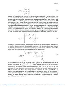
Dislocation Intersections
i. ZnSe/GaAs(1 00) average strain model •
103
102 102
103
104
log(h/b) Figure 5. Observed spacingjof misfit dislocations in (110) and (110) directions vs. film thickness (adapted from Reference 26). The curve is a prediction based on average strain in the film, neglecting det
Data Loading...