Relaxation of SiGe Films for the Fabrication of Strained Si Devices
- PDF / 544,178 Bytes
- 6 Pages / 612 x 792 pts (letter) Page_size
- 101 Downloads / 306 Views
G1.4.1
RELAXATION OF SiGe FILMS FOR THE FABRICATION OF STRAINED Si DEVICES J.S. Maa, D. J. Tweet, J.J. Lee, S.T. Hsu, K. Fujii*, T. Naka*, T. Ueda*, T. Baba*, N. Awaya* and K. Sakiyama*, Sharp Labs of America, Camas, WA and IC Group*, Sharp Corporation, Tenri, Japan ABSTRACT For the fabrication of bulk strained Si devices, a thin Si layer is deposited on a virtual substrate consisting of a several µm thick compositionally graded SiGe layer. A simpler approach utilizing H or He implantation to enhance relaxation of a thin SiGe film was recently reported. In this current work, hydrogen implantation is used to enhance the SiGe relaxation; and, relaxation beyond the previous reported limit is demonstrated. Experiments are performed on CVD deposited SiGe films with Ge fractions ranging from 20% to 40 % and thickness in the range of 100nm to about 500nm. After annealing at 800°C, relaxation of more than 80% is achieved. PMOS and NMOS devices are successfully fabricated and much enhanced hole and electron mobilities are demonstrated. INTRODUCTION Carrier transport enhancement by the use of a strained-Si channel has drawn much attention recently since it leads to a CMOS technology with improved speed or reduced power on the same technology node [1,2]. In order to achieve tensile strain in the thin Si channel a SiGe virtual-substrate is used. The SiGe virtual-substrate is fabricated by a thick relaxed SiGe layer of constant Ge concentration on a thick layer of SiGe with graded Ge composition deposited on a Si substrate. The total SiGe thickness is on the order of several microns [3]. An alternative method for forming a relaxed virtual-substrate is to start with a comparatively thin SiGe film and enhance the relaxation by hydrogen implantation and annealing [4,5]. Hydrogen implantation was successfully used to induce exfoliation of silicon for the fabrication of high-quality silicon-on-insulator (SOI) wafers. However, it was previously reported hydrogen was not as effective as helium to induce SiGe relaxation. In order to achieve 80% relaxation of a SiGe layer with 30% Ge, He implantation was required [6]. The goals of this work are twofold: (1) to produce a 300-500nm relaxed SiGe film with surface Ge content >30% by hydrogen implantation enhanced relaxation, and (2) to fabricate strained Si device on this relaxed SiGe substrate.
EXPERIMENTAL 6-inch N-and P-type Si (100) wafers are used as substrates for SiGe deposition. Prior to deposition, the wafers are dipped in dilute HF to remove the native oxide. After a
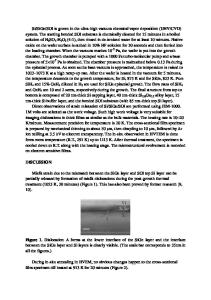
Data Loading...