Dislocation Nucleation, Growth and Suppression During CW Laser Annealing of Silicon
- PDF / 3,034,537 Bytes
- 7 Pages / 415.8 x 637.2 pts Page_size
- 2 Downloads / 321 Views
DISLOCATION NUCLEATION, OF SILICON
193
GROWTH AND SUPPRESSION DURING CW LASER ANNEALING
G.A. ROZGONYIa*, H. BAUMGARTa AND F. PHILLIPPb a) Max-Planck-Institut fhr Festk6rperforschung, b) Max-Planck-Institut fUr Metallforschung Heisenbergstr. 1, D-7000 Stuttgart 80 Federal Republic of Germany
ABSTRACT
Optical, X-ray and transmission electron microscopy plus preferential chemical etching have been used to examine the dislocations and lattice strain introduced during cw laser annealing of silicon. In addition to a substrate scanning mode we operate our cw Ar-ion laser in a "pulse" mode by using an electronically activated shutter located within the laser cavity. This permits accurate measurements to be made on isolated spots or large area scans with a dislocation density that can be deliberately varied. In particular we discuss surface slip traces, their component dislocations and resulting lattice strains, as well as submicron extrinsic dislocation loops which result from the condensation of ion-implantation produced interstitial silicon. Recommendations are presented for producing defect and strain-free material, as well as samples with specific densities of dislocations.
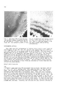
Laser annealing studies have matured rapidly as a result of the burst of activity following the USA-USSR seminar on ion-implantation held in Albany in 1977. Not only have many areas of technological interest been explored, but also fundamental aspects of crystal growth under highly non-equilibrium thermodynamic conditions can now be systematically investigated. Our own interest in the nucleation, characterization and ultimately the suppression of defects have been well served by using a cw Ar-ion laser to deliberately introduce dislocations by inserting an electromechanical shutter inside the cavity of a cw Ar1 ion laser( ). Variation of the shutter speed from 5 to 1000 ms and adjustment of the laser power from 5 to 10 W enabled isolated spots of 40 to 80 im in diam to be obtained with slip dislocation densities from zero to 106 cm- 2 (2). Large area samples could also be prepared, with or without slip, see Figs. la and b, respectively, by scanning the substrate in a step and repeat fashion with a programable substrate position controller. Because the laser dwell time could be controlled either by use of the shutter or by rapidly scanning the substrate it was not necessary to heat the wafers in order to suppress the formation of slip dislocations. Details of the distribution and surface morphology of the dislocations were obtained by Nomarski Differential Interference Contrast Microscopy (N-DIC) coupled with preferential chemical etching; the character and subsurface microstructure of the dislocations were determined by high voltage transmission electron microscopy (HVEM) in an Hitachi HU650 operating at 600 keV; while lattice strains were revealed by X-ray topography (XRT).
on leave from Bell Laboratories,
Murray Hill, NJ 07974
194
AND".
Fig. 1 N-DIC optical micrographs of large area step-scanned cw laser annealed samples (a) with, and
Data Loading...