CW Laser Annealing of Ion Implanted Oxidized Silicon Layers on Sapphire
- PDF / 342,391 Bytes
- 6 Pages / 420.48 x 639 pts Page_size
- 115 Downloads / 341 Views
G. ALESTIG, G. HOLMEN AND S. PETERSTREM Department of Physics, Chalmers University of Technology, Sweden
S-412 96 Gbteborg,
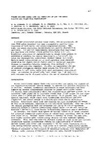
ABSTRACT CW laser annealing has been performed on silicon on sapphire (SOS) implanted with boron or phosphorus ions to a dose of 1015 2 ions/cm . The laser irradiation was done both with and without an oxide layer on top of the silicon and from both the silicon and the sapphire side. Sheet resistivity and Hall effect measurements were used for the analysis of the samples. Good annealing and high activation of the dopants were obtained for both oxidized and unoxidized SOS. For samples irradiated from the silicon side, the needed laser power changed depending on the thickness of the oxide. For samples irradiated from the sapphire side, the needed laser power was independent of oxide thickness.
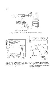
INTRODUCTION Silicon on sapphire (SOS) is an interesting material for the fabrication of electronic devices. If ion implantation is used as a doping method, the crystal structure must be restored and the dopants activated by a post-implantation annealing process. In recent years, the use of laser or electron beams for annealing of semiconductors has attracted much attention [1]. However, relatively few investigations of SOS annealed in this way have been made [2-4]. In this work we report on scanned CW (continuous wave) laser annealing of boron or phosphorus implanted SOS. Since most device processing techniques incorporate the use of SiO2 on Si, we have studied annealing of samples with an oxide overcoat as well as samples without oxide. A unique feature of silicon on sapphire is the possibility of laser annealing from the sapphire side. This would make it possible to anneal areas otherwise masked by contacts etc. In the work presented here, we have performed both back side and front side laser annealing. Sheet resistivity measurements were used for the analysis of the samples. On some samples Hall effect measurements were made.
EXPERIHENTAL PROCEDURE The material used in the investigations was intrinsic (> 50 Qcm), 0.6 pm (100) siliconon sapphire. The thickness of the sapphire was 0.33 mm. Since some of the samples were to be irradiated from the sapphire side, the SOS wafers were purchased with a back side optical polish. Prior to the ion implantation, the silicon on some of the wafers was oxidized in dry oxygen at 1100 0 C. Three different oxide thicknesses were grown; 490 A, 830 A, and 1190 A. The samples were then implanted using the Chalmers 400 kV ion accelerator with either 1015 11
B ions/cm2 at 150 keV or 10 15
31
p ions/cm2 at 250 key.
The implantations were
performed at 100 off the surface normal and at room temperature. 2 After the implantations, the samples were cut into pieces measuring 7x 7 mm and laser annealed with a CW Ar ion laser, operating in the TEMoo mode on the 5145 A line. Focusing was obtained with a 100 mm focal length lens, giving a 2 calculated beam spot diameter of 34 Pm (at l/e intensity points) E5]. The Mat. Res.
Soc. Symp. Proc. Vol. 13 (1983) @Elsevier science Pu
Data Loading...