Dislocation reduction with quantum dots in GaN grown on sapphire substrates by molecular beam epitaxy
- PDF / 1,056,295 Bytes
- 6 Pages / 595 x 842 pts (A4) Page_size
- 21 Downloads / 365 Views
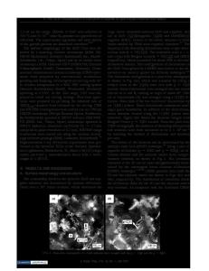
Dislocation reduction with quantum dots in GaN grown on sapphire substrates by molecular beam epitaxy David J. Smith,1 Daming Huang,2 Michael A Reshchikov,2 Feng Yun,2 T. King,2 Hadis Morkoç,2 and Cole W Litton3 1 Arizona State University, Tempe, AZ 85287-1704 2 Virginia Commonwealth University, Richmond, VA 23284-3072 3 Air Force Research Laboratory (AFRL/MLPS), Wright Patterson AFB, OH 45433 ABSTRACT We have investigated a novel approach for improving GaN crystal quality by utilizing a stack of quantum dots (QDs) in GaN grown on sapphire substrates by molecular beam epitaxy. The GaN films were grown on GaN/AlN buffer layers containing multiple QDs and characterized using x-ray diffraction, photoluminescence, atomic force microscopy, and transmission electron microscopy. The density of the dislocations in the films was determined by defect delineation wet chemical etching and atomic force microscopy. It was found that the insertion of a set of multiple GaN QD layers in the buffer layer effectively reduced the density of the dislocations in the epitaxial layers. As compared to a density of ~1010 cm-2 in typical GaN films grown on AlN buffer layers, a density of ~3x107 cm-2 was demonstrated in GaN films grown with the QD layers. Transmission electron microscopy observations confirmed termination of threading dislocations by the QD layers. INTRODUCTION III-nitride semiconductors have a wide range of applications in blue/UV light-emitters and detectors, and high power amplifiers [1]. Nitride films are most commonly grown on foreign substrates such as sapphire. However, the large difference in lattice constant between the IIInitrides and the sapphire substrate, and the lack of a common stacking sequence result in high defect densities in the epilayers. The typical dislocation density in a ~1 µm GaN film grown on AlN buffers or directly on sapphire substrates is on the order of 109 cm-2 or higher [2]. Great strides have been made to reduce defect densities in GaN films by growing on native substrates [3]. Since native substrates are not readily available in sufficient size and quantity, alternative methods using various types of buffer layers, such as multiple low temperature AlN or GaN layers inserted in high temperature GaN layers have been investigated for MOCVD growth [4]. In this paper, we report the improvement of GaN crystal quality obtained by utilizing a stack of GaN quantum dots (QDs) as buffer layers grown on sapphire substrates by molecular beam epitaxy (MBE). The GaN films grown on GaN/AlN buffer layers containing multiple QDs were characterised by x-ray diffraction (XRD), photoluminescence (PL), defect delineate chemical etching, atomic force microscopy (AFM), and transmission electron microscopy (TEM). The results were also compared to those obtained from samples grown without using any QDs as part of the buffer layer. EXPERIMENTAL Sample growth The samples used in this investigation were grown on c-plane sapphire substrates by MBE with both ammonia and radio-frequency-activated nitrogen sources. Two sets
Data Loading...