InNAs and GaInNAs self-assembled quantum dots and lasers grown by solid source molecular beam epitaxy
- PDF / 397,465 Bytes
- 6 Pages / 612 x 792 pts (letter) Page_size
- 19 Downloads / 460 Views
T3.31.1
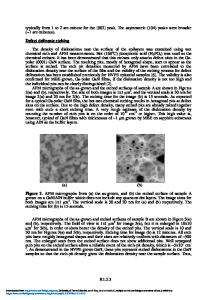
InNAs and GaInNAs self-assembled quantum dots and lasers grown by solid source molecular beam epitaxy Z.Z. Sun, S.F.Yoon, K.C. Yew, and B.X. Bo School of Electrical and Electronic Engineering, Nanyang Technological University, Nanyang Avenue, Singapore 639798, Rep. Of Singapore ABSTRACT Self-assembled Ga1-xInxNyAs1-y quantum dots were grown on GaAs by solid source molecular beam epitaxy (SSMBE). Introduction of N was achieved by a RF Nitrogen plasma source. Formation of quantum dots by S-K growth mode is confirmed by observation of standard 2D-3D RHEED pattern transition. Atomic force microscopy (AFM) and photoluminescence (PL) measurements were used to characterize the structure and optical properties of GaInNAs quantum dots. High GaInNAs quantum dot density (1010~1011cm-2) was obtained for different In and N composition (0.3≤ x ≤1, y≤0.01). The effect of surface coverage on dot density, dot size, and optical properties was studied in detail. Adjusting the bandgap confinement by incorporating a GaNAs strain-reduction layer into the GaInNAs dot layer was found to extend the emission wavelength by 170nm. Room temperature pulsed operation is demonstrated for a Ga0.5In0.5N0.01As0.99 quantum dot laser emitting at ~1.1µm. INTRODUCTION Considerable attention has been devoted to achieve long wavelength lasers (1.3µm and 1.55µm for optical communication application) on GaAs substrates. The main motivation behind this is reduction in production cost due to the cheaper and more robust GaAs substrates (compared to InP substrates), and good compatibility with GaAs/AlAs distributed Bragg reflectors for GaAs-based vertical cavity surface emitting lasers. So far, success has been limited to two methods; one method involves using self-assembled (Ga)InAs quantum dot (QD) structures, and another involves using quantum well (QW) structures of dilute nitrides such as GaInNAs. Quantum dots formed by 3D-growth of high-strained GaInAs is helpful to extend the wavelength, and improve laser properties due to the δ-shaped density of states of QDs [1]. A 1.3µm GaAs-based QD laser has been achieved using GaInAs QDs [2,3] or combined InAs/Ga(In)As QDs [4,5,6] in the active region. Recently, GaInNAs is proving to be a very promising material for application in 1.3-1.55µm laser diodes. The introduction of N into Ga(In)As effectively reduces the energy bandgap due to the large bowing coefficient between GaN and GaAs [7]. GaInNAs/GaAs QW lasers emitting at 1.3µm [8,9] and 1.52µm [10] have been reported. Recently, self-assembled GaInNAs/GaAs quantum dot structures have been proposed to achieve long-wavelength emission [11,12,13]. PL emission up to 1.52µm has been observed from Ga0.3In0.7N0.04As0.96 QDs grown by gas source molecular beam epitaxy (GSMBE) [11]. Although the spectrum was relatively weak and broad, it demonstrated the possibility of using QDs for long wavelength tuning. Furthermore, it was reported that N incorporation usually results in several times higher dot density compared to In(Ga)As dots grown under identical
T3.31.2
Data Loading...