Dry Etching Damage Effect on Ohmic Characteristics of GaN
- PDF / 330,859 Bytes
- 5 Pages / 414.72 x 648 pts Page_size
- 92 Downloads / 351 Views
in various conditions. The sheet resistance of InN, InGaN, and InAIN was found to increase after the layers were exposed to an Ar plasma under both ECR-RIE and conventional RIE conditions. Another method to investigate the dry etching damage effect is reported by Ping et al.[ 11]. They fabricated the Schottky contact on etched surface to investigate the diode characteristics, and this technique is highly sensitive to induced defects and thus has been utilized extensively for GaAs and other 1HI-V compounds. In this paper, we present the electrical characteristics of GaN surfaces etched with ICP-RIE and CAIBE. ICP-RIE and CAIBE were performed in C12 and H 2 gas plasmas. Using transmission line method, the current-voltage(I-V) characteristics, the contact resistance, the sheet resistance and the specific contact resistivity of the samples etched with various conditions are presented. The photoluminescence(PL) spectra were measured at 17K and room temperature, and Auger electron spectroscopy(AES) and x-ray photoelectron spectroscopy(XPS) are used to investigate the surface stoichiometry and the induced damage of the samples. EXPERIMENTS The GaN epilayers used for this study were grown on (0001) sapphire substrates by metalorganic chemical vapor deposition(MOCVD). A GaN buffer layer of 250 A was grown at 500 'C followed by the growth of 2-pm thick GaN. The carrier concentrations of the GaN layers, measured by Hall measurement, were -7 X 10¹⁷/cm 3 . After the samples were etched to form the TLM mesa pattern using ICP-RIE and CAIBE with C12 and Ar, the samples were slightly etched with C12 gas, C12:H2=1:1 gas, and H 2 gas for 3 minutes in order to induce the damage to the surface of the samples, respectively. The rectangular pads were 200.tm wide and 100ptm long. The separation of the 7 contact pads of TLM patterns were between 5um and 30[tm in Sum increment. We evaporated Ti/Al/Ni/Au=150/2700/400/4000 A on the samples for contact metal using e-beam evaporator with a base pressure of < 5 X 10⁻⁷ torr. Before evaporating the contact metal, the samples were immersed in a HCI:H 20= 1:1 solution for 30seconds followed by deionized water rinse for 10 minutes. After the contact metal evaporation, the contact pads are defined by a conventional lift-off process and annealed at 700 'C for Iminute using rapid thermal annealer(RTA). We measured the I-V characteristics of the TLM metal contacts using a 4-point probe with HP 4145B analyzer. We measured the PL, the XPS, and the AES of the etched surface to investigate the damage effect induced by dry etching. RESULTS & DISCUSSION
\
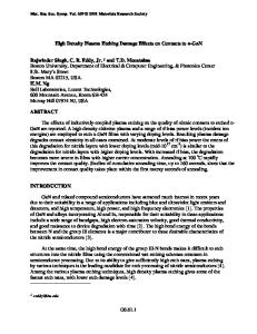
&bsrafe Tenr=2w =oc
30
•
0,B
Su :s neTenp.T=100'C
2500-
~0,6
200D-
0
2
40
HJ
60
(
80
100
0
20
9/6) )
aH
GaO
a
0.00
0-
40
60
80
H/(CI2+H2)(%)
(a) Etch rate
(b) OES of etch products
Figure 1. Etch rate of GaN and OES of etch products 496
100
C12 and their compound chemical gases are widely used as etch chemistries of HI- V nitrides and the other HI-V compound semiconductors for their higher volatility of mH-chlorides than that
Data Loading...