Effect of magnetic field on the formation of macroporous silicon: structural and optical properties
- PDF / 348,209 Bytes
- 6 Pages / 432 x 648 pts Page_size
- 86 Downloads / 354 Views
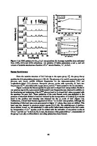
Effect of magnetic field on the formation of macroporous silicon: structural and optical properties E. E. Antunez1, J. O. Estevez2, J. Campos3, M. A. Basurto1, V. Agarwal1* 1 Centro de Investigación en Ingeniería y Ciencias Aplicadas, UAEM, Av. Universidad 1001, Col. Chamilpa, Cuernavaca, Morelos, CP 62210, México. 2 Instituto de Física, B. Universidad Autónoma de Puebla, A.P. J-48, Puebla 72570, México. 3 Instituto de Energías Renovables, UNAM, Priv. Xochicalco S/N, Temixco, Morelos 62580, México. ABSTRACT The conventional method to fabricate porous silicon with n-type substrates requires light assisted generation of holes used in the electrochemical reaction. Recently, two different methods have been proposed to fabricate some similar structures: Hall effect [1] and lateral electrical field [2]. Hall effect assisted etching involves the application of a perpendicular electric and magnetic field to achieve the concentration of holes at the HF/silicon interface to assist the electrochemical reaction, while the other involves the application of a lateral electrical field across the silicon wafer. In this work, the electrochemical etching of high resistivity n-type silicon wafers under the combined effect of magnetic and lateral electrical field to produce photoluminescent macroporous structures under dark conditions, is reported. A lateral gradient in pore sizes as well as in light emission is observed. Optical and structural properties were studied for their possible applications as a biosensor. INTRODUCTION Electrochemical anodisation is the most commonly used technique for the fabrication of porous silicon (PSi). It is well known that in order to carry out an anodic oxidation at the HF/silicon interface and consequently PSi formation, the presence of holes is required to assist the electrochemical reaction. For p-type Si, the majority charge carriers are holes, and etching process is not limited by their availability, so p-type porous silicon (p-PSi) layers are easily produced. On the other hand, light assisted anodisation (where illumination of the wafer helps in the generation of the required holes) is a conventional technique for obtaining PSi from n-type silicon wafers [3-4]. However, light assisted etching is depth limited. Recently, Lin et al.[1] proposed a new method for fabricating photoluminescent structures in n-type Si under dark conditions (without light assistance), using Hall effect which involves the application of perpendicular electric and magnetic fields, to drive holes to the HF/silicon interface. Li et al. [2], on the other hand, reported macropore formation by applying a lateral electrical field, which results in a current flow across the substrate, producing photoluminescent n-PSi in the dark. However, it is well known that PSi has a large range of morphologies. The macroporous silicon (MPSi) morphology is strongly dependent on the doping type level of the Si substrate and the electrochemical etching parameters [5]. One of the main applications of PSi based optical devices is biosensing, and
Data Loading...