Effect of MeV Si Ion Bombardment on Thermoelectric Characteristics of Sequentially Deposited SiO2/AuxSiO2(1-x) Nanolayer
- PDF / 128,744 Bytes
- 6 Pages / 612 x 792 pts (letter) Page_size
- 80 Downloads / 335 Views
0929-II04-10
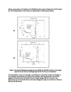
Effect of MeV Si Ion Bombardment on Thermoelectric Characteristics of Sequentially Deposited SiO2/AuxSiO2(1-x) Nanolayers S. Budak1, B. Zheng1, C. Muntele1, Z. Xiao2, I. Muntele1, B. Chhay1, R. L. Zimmerman1, R. L. Holland1, and D. Ila1 1 Physics/CIM, Alabama A&M University, 4900 Meridian Street P.O. Box 1447, Normal, AL, 35762 2 Electrical Engineering, Alabama A&M University, 4900 Meridian Street, Normal, AL, 35762 ABSTRACT We made an electro-cooling superlattice system consisting of 50 and 100 periodic nanolayers of SiO2/AuxSiO2(1-x) with Au layers deposited on both sides as metal contacts. The deposited multi-layer films have an alternating layers of 10 nm thick. The ultimate objective of this research is to tailor the Figure of Merit of layered structures used as thermoelectric generators. The superlattices were then bombarded by 5 MeV Si ions at three different fluences to form nano-cluster structures. The film thicknesses and stoichiometry were monitored by Rutherford backscattering spectrometry (RBS) before and after MeV ion bombardments. We measured the thermoelectric efficiency of the fabricated device before and after the MeV ion bombardments. We measured the cross plane thermal conductivity by the 3rd harmonic method, the cross plane Seebeck coefficient, and the electrical conductivity using the Van Der Pauw method before and after the 5 MeV Si bombardments.
INTRODUCTION
Thermoelectric materials are important due to the interest in their applications in thermoelectric
power
generation
and
microelectronic
cooling
[1].
Effective
thermoelectric materials have a low thermal conductivity and a high electrical conductivity [2]. The performance of the thermoelectric materials and devices is shown by a dimensionless Figure of Merit, ZT = S 2σT / κ , where S is the Seebeck coefficient,
σ is the electrical conductivity, T is the absolute temperature, and κ is the thermal conductivity [3]. ZT can be increased by increasing S, increasing σ, or decreasing κ.
In this study we report on the growth of a SiO2/AuxSiO2(1-x) Superlattice on the silica and silicon substrates using an ion-beam assisted deposition (IBAD) system, and high energy Si ion bombardments of the films for reducing thermal conductivity and increasing electrical conductivity.
EXPERIMENTAL
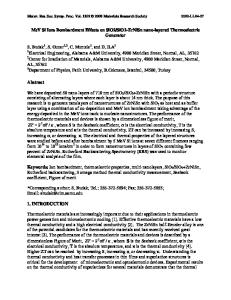
We have grown SiO2/AuxSiO2(1-x) superlattice nanolayer films on the silica and silicon substrates with the IBAD system. The multilayer films were sequentially deposited to have a periodic structure consisting of alternating SiO2 and AuxSiO2(1-x) layers. The two electron-gun evaporators for evaporating the two solids were turned on and off alternately to make multilayers. The thickness of the layers was controlled by an INFICON deposition monitor. The film geometry used in this study is shown in Fig.1. The geometry in Fig.1 shows two Au contacts on the top and bottom of the multilayers. These contacts were used in the Seebeck coefficient measurement system.
The electrical conductivity was measured by the Van der Pauw system and the thermal c
Data Loading...