Improvement on Thermoelectric Characteristics of Layered Nanostructure by Ion Beam Bombardment
- PDF / 122,654 Bytes
- 8 Pages / 612 x 792 pts (letter) Page_size
- 11 Downloads / 280 Views
0929-II04-12
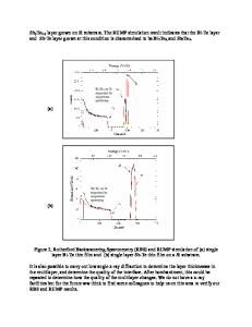
Improvement on Thermoelectric Characteristics of Layered Nanostructure by Ion Beam Bombardment B. Zheng, S. Budak, C. Muntele, Z. Xiao, S. Celaschi, I. Mutele, B. Chhay, R. L. Zimmerman, L. R. Holland, and D. Ila Center for Irradiation of Materials -Alabama A & M University, P.O.Box 1447, Normal, AL, 35762 ABSTRACT We made an n-type nanoscale multilayer superlattice thermoelectric cooling device which consists of multiple periodic layers of Si 1-x Ge x / Si, The thickness of each layer ranges between 10 and 50 nm. The super lattice was bombarded by 5 MeV Si ions with different fluence in order to form nanoscale cluster quantum dot structures. We measured the thin film cross plane thermal conductivity with 3ω method, measuring the cross plane Seebeck coefficient, and finally measuring the cross plane electric conductivity before and after ion bombardment. As predicted, the thermo-electric figure of merit of the films increases with the increase of Si ion fluence. In addition to the effect of quantum well confinement of the phonon transmission, the nano-scale crystal quantum dots produced by the incident Si ion beam further adversely affect the thermal conductivity. The defect and disorder in the lattice caused by bombardment and the grain boundary of Metal Cu Heats up Q these nano-scale cluster increase scattering of phonon and increase the chance of the 10nmSi Ge /10nm Si inelastic interaction of phonon and 70 layers n type SL annihilation of phonon, this limits phonon mean free path, phonons are chiefly absorbed and dissipated along the lattice, Q Cool down Metal Cu therefore reduces the cross plane thermal SiO conductivity, The increases of the electron density of state in the miniband of Si substrate nanoscale cluster quantum dot structure formed by bombardment also increases Fig. 1. Schematic of Si 1-x Ge x / Si superlattice TE device Seebeck coefficient, and the electric conductivity. Eventually, the thermo-electric figure of merit of the films increases. 1-x
x
2
INTRODUCTION Si / Si1-x Gex multiplayer superlattice thin film thermo-electric (TE) cooling devices was made in CIM as shown in Fig. 1. This thin films is a periodic quantum well structure consisting of tens to hundreds of alternating layers with different band gap (Si: 1.12 eV, Si 1-x Ge x : 0.8∼0.9 eV), The thickness of each layer ranges between 10 and 50 nm. The performance of superlattice thin film thermoelectric device is quantified by the
dimensionless figure of merit ZT = S2 σT/ k. Our aim is to obtain high ZT values by increasing the Seebeck coefficient S and the electrical conductivity σ, and reducing the thermal conductivity k by bombarding the superlattice structure with MeV Si ion. The bombardment tends to form nanoscale cluster of quantum dot structures. In addition to the quantum well confinement of the phonon transmission due to Bragg scattering and reflection at lattice interface [1, 2, 3], the defect and disorder in the lattice caused by bombardment and the grain boundary of these nanoscale cluster formed by bombardm
Data Loading...