Effect of Plasma Damage on Interface State Density Between a-Si:H and Insulating Films
- PDF / 405,405 Bytes
- 6 Pages / 414.72 x 648 pts Page_size
- 69 Downloads / 294 Views
Downloaded from https://www.cambridge.org/core. Columbia University Libraries, on 14 Aug 2019 at 01:47:49, subject to the Cambridge Core terms of use, available at https://www.cambridge.org/core/terms. https://doi.org/10.1557/PROC-377-9
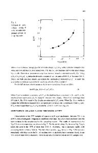
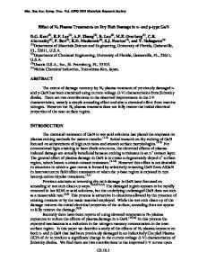
surface of a-Si:H. EXPERIMENTAL Samples were prepared by rf plasma-assisted chemical vapor deposition (P-CVD) in a capacitive reactor. The gas compositions to deposit different layers were SiH 4(25sccm) and H2(25sccm) for a-Si:H, SiH4(5sccm) and NH 3(150sccm) for a-SiN, 7 :H, and SiH 4(3sccm) and N20(240sccm) for SiOC0 :H. The temperature of the substrate was maintained at 2500 C and the total gas pressure in the reactor was 0.Sorr. The substrate of the film was Corning 7059 glass. Thickness of each layer was controlled by deposition time to be 21nm for the a-Si:H layer, 13nm for the a-SiN 1 .7:H layer and 17nm for the a-SiOz0 layer. Plasma-treated samples were prepared by plasma discharge of NH3 or N 20 gas on a-Si:H surface. The condition of plasma discharge was the same as that for the deposition of a-SiN, 7 :H or a-SiOC:H except for no introduction of SiH 4 gas; The gas flow rate was 150sccm for NH43 or 240sccm for N20 under the pressure of 0.5 torr. All samples except for the a-Si:H, a-SiN1 .7:H and a-SiOj 0 films were passivated by the a-SiN1 .7:H layer to prevent from oxidation in the air. The structures of typical samples are shown in Fig.1 and all samples we prepared are listed in Table I. In the present paper, A/B indicates A on B structure and interface A/B indicates interface between A layer and B layer. The Symbol C*/A indicates plasma discharge of C gas on the surface of A layer. During the experiment, we found that some samples have similar shape and intensity. The spectra were grouped to A, B, C and D which have similar PD spectra to samples (a), (b), (c) and (d), respectively. These groups are listed in Table I. RESULTS The layered effects of a-SiN,.7:H/a-Si:H/7059 and a-SiO2.Wa-Si:H/7059 are shown in Fig.2. The sub-gap absorption appeared in the energy region below the Urbach tail is recognized to be due to bulk and interface defects. When the thicknesses of films are several tens of nanometer, predominant defects are not originated from the bulk but from the interface.') Therefore, the sub-gap absorption is owing mainly to the interface defects in our experimental condition. A peak at 0.88eV in Fig.2 is the O-H vibration in the substrate.') The absolute value of PD magnitude differs from run-to-run measurements due to a change in the setting of optical alignment. The relative magnitude of PD signal was fitted by using O-H absorption of substrate. The dotted line in Fig.2 shows the PD signal of the 7059 substrate. PD signal below photon
4-ii.: (a)
7
3nm
40
____
(c)
(b)
Fig. 1 Structures of the samples. (a) a-Si:H/7059 (b)a-SiN1 .7:HFa-Si:H/7059 (c)a-SiO2.0/a-Si:H/7059.
10
Downloaded from https://www.cambridge.org/core. Columbia University Libraries, on 14 Aug 2019 at 01:47:49, subject to the Cambridge Core terms of use, available at https://www.cambridge
Data Loading...