Effect of the duration of the growth process on the properties of GaN grown by the sublimation method
- PDF / 213,104 Bytes
- 3 Pages / 612 x 792 pts (letter) Page_size
- 0 Downloads / 360 Views
ICATION, TREATMENT, AND TESTING OF MATERIALS AND STRUCTURES
Effect of the Duration of the Growth Process on the Properties of GaN Grown by the Sublimation Method A. A. Wolfson and E. N. Mokhov^ Ioffe Physicotechnical Institute, Russian Academy of Sciences, St. Petersburg, 194021 Russia ^e-mail: [email protected] Submitted May 13, 2008; accepted for publication, May 21, 2008
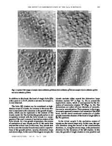
Abstract—Variation in the structural and morphological features and luminescent characteristics of thick epitaxial GaN layers grown by the sublimation sandwich method with the duration of the crystallization process has been studied. This was, in particular, done by means of scanning electron microscopy in the secondary-electron and color-cathodoluminescence modes. It was found that rather high-quality GaN layers with a thickness of up to 0.5 mm can be grown in a time of about 1.5 h, with their surface hardly exhibiting any luminescence in the visible spectral range. However, making the growth process longer in order to obtain thicker layers impairs the quality of a crystal being grown, which is accompanied by an increase in the intensity of cathodoluminescence from its surface layer in the visible (predominantly yellow) region of the spectrum. Reasons for the poorer quality of GaN layers in this case are discussed. It is suggested that, as the evaporation rate from the source decreases, the amount of active nitrogen near the growth surface becomes lower. PACS numbers: 81.05.Ea, 81.10.Bk, 78.60.Hk DOI: 10.1134/S1063782609030269
1. INTRODUCTION
2. EXPERIMENTAL
It is known that GaN is one of the most promising wide-gap semiconductor materials used to develop optoelectronic devices and, in particular, high-efficiency short-wavelength lasers for optical-memory systems [1]. However, a serious obstacle in the way of improving devices of this kind is the lack of sufficiently perfect GaN substrates suitable for fabrication of various epitaxial structures. Undoubtedly, the best substrates for this purpose are wafers of GaN itself. Therefore, such close attention is being given to growth of bulk GaN crystals to be used as substrates for growth of GaN layers or GaN-based solid solutions.
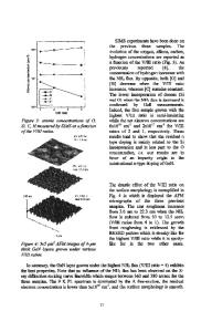
GaN was grown by the sublimation sandwich method in which a substrate and a source, spaced by a narrow clearance of about 3–5 mm (Fig. 1), were heated in a temperature field with an axial gradient, with the source temperature exceeding the substrate temperature by several tens of degrees. The growth was performed on a SiC or sapphire substrate in a flow of ammonia at temperatures of 1100–1250°C. A GaN powder served as the vapor source. The growth rate was varied within the range 50–400 µm/h, with the thickness of the layers being 70 to 1200 µm. The duration of the growth process was in the range from 15 min to several hours.
Several methods for the growth of bulk GaN crystals are known, one of these being the sublimation sandwich method [2] employed in this study. This promising technique enables growth of bulk GaN crystals at growth rates as high as 1 mm/h [3].
T
Data Loading...