The Effect of Al in Plasma-Assisted MBE-Grown GaN
- PDF / 263,405 Bytes
- 6 Pages / 612 x 792 pts (letter) Page_size
- 21 Downloads / 318 Views
W3.36
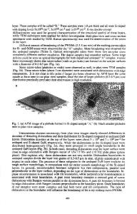
(Al2O3), cut along the (0001)-plane, with a 0.5 µm thick Ti-layer on the backside and the growth temperature was measured by a pyrometer. Before insertion into the MBE-system the substrates were ultrasonically degreased in trichloroethylene, acetone and methanol and etched for 15 min at 48 °C in a mixture of HCl:H3PO4 (3:1). In the growth chamber the samples were first outgassed at 700 °C for 30 minutes, and thereafter nitridised by exposure to active nitrogen for another 30 minutes. At the same temperature a 110 nm thick GaN buffer-layer was subsequently grown at low growth rate 0.15 µm/h and with minimum nitrogen flow (0.6 sccm) and power (200 W) in order to maintain the RFplasma of the nitrogen source. A (2x2) reconstruction pattern was obtained after a few minutes growth of the buffer layer, and this surface periodicity remained throughout the whole deposition. We denote the dilute AlxGa1-xN alloy layers by (Al)GaN which are intermediate between normal alloys with x > 1% and isoelectronically doped layers, GaN:Al with x < 10-4. The (Al)GaN bulk layer was grown (with the Al shutter open) using a nominal Ga-flux corresponding to a growth rate of 1 µm/h. The growth temperature was 750 °C, and RF-power and N2-flux were 600 W and 3.0 sccm, respectively. The (2x2) reconstruction has been taken as a proof of a Ga-rich growth [7]. For a growth time of 1 h, cross-sectional SEM investigations indicated a thickness of only 600 - 700 nm which is a result of Ga desorption. A measure of the Al-concentration in the samples was made by SIMS, using the peak intensity ratio between the Al and Ga-signals. The relation between the SIMSsignal and the Al-composition provided by the MBE-growth was fairly linear. The absolute calibration of about 3% Al in GaN was made by AES through the intensity ratio of the AlKLL and GaLMM peaks. This value was used as the calibration value for the SIMS results. The AES was made with a Perkin-Elmer Physical Electronics PHI 590 equipment. An electron accelerating voltage of 3 keV at 1.5 µA beam current provided an analysis spot size of 3 µm. For the PL investigation the samples were mounted on the cold finger of a closed cycle Cryogenic Lab System, CSW-204SLB cryostat, allowing the temperature to be varied between 6.5 and 350 K. The excitation was made by a Liconix He-Cd UV laser, giving a typical power of 25 mW at a wavelength of 325 nm. The monochromator was a Spex 270M single grating monochromator with a Photometrix AT200 CCD camera as detector. Hall effect measurements were obtained using 3x3 mm samples in the van der Pauw geometry. The contacting material was In and the contacts were annealed at 425 °C for 2 minutes. To characterise the sample surfaces a JEOL JSM-6301F scanning electron microscope was used. RESULTS Low-temperature PL-spectra (at 6.5 K) from two representative samples are shown in Figure 1. The upper spectrum is from pure GaN while the other is from (Al)GaN. The peak is non-symmetric with a low-energy tail, which is reduced with Al-concentration. The spectra have a typical
Data Loading...