Effects of Hydrogen Annealing Process Conditions on Nano Scale Silicon (011) Fins
- PDF / 1,159,006 Bytes
- 5 Pages / 612 x 792 pts (letter) Page_size
- 71 Downloads / 279 Views
J3.1.1
Effects of Hydrogen Annealing Process Conditions on Nano Scale Silicon (011) Fins Rownak J. Zaman1, Weize Xiong2, Rudy Quintanilla1, Thomas Schulz3, C. Rinn Cleavelin2, Rick Wise2, Mike Pas2, Paul Patruno4, Klaus Schruefer3 and Sanjay K. Banerjee5 1 ATDF, 2706 Montopolis Drive, Austin, TX 78741, USA 2 SiTD, Texas Instruments Inc., 13560 North Central Expressway, Dallas, TX 75243, USA 3 Infineon Technologies, München, Germany 4 SOITEC USA, 2 Centennial Drive, Peabody, MA 01960, USA 5 University of Texas at Austin, Microelectronics Research Center, Austin, TX 78758, USA
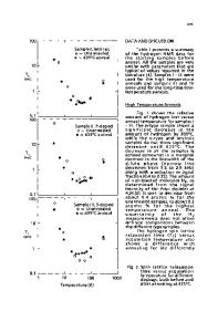
ABSTRACT In this paper we present a comprehensive study of the impact of the Hydrogen (H2) annealing conditions on nano scale silicon fin structures. Hydrogen pressure was varied from 15Torr to 600Torr and anneal temperature was varied from 600oC to 900oC. We found H2 annealing can cause faceting, corner rounding and smoothing of the etched silicon surfaces. The degree of the fin transformation is a function of both pressure and temperature. Furthermore, low pressure and high temperature enhance the silicon movement and can cause damage to the nano scale fins.
INTRODUCTION MuGFET (Multi-Gate Field Effect Transistor) devices (FinFET [1], Tri-gate [2], Pi-Gate [3] and Omega Gate [4]) are promising structures that could extend CMOS scaling to beyond the 22nm node [5]. The key feature of MuGFET device structures is the nano scale silicon fins. Unlike planar bulk CMOS, where current conducts on the top surface of the silicon wafer, carrier transport in MuGFET devices takes place not only on the top surface in the case of Tri-gate devices, but also along the sidewalls of etched fins. These etched surfaces are inherently rough. Such rough surfaces reduce carrier mobility and raise concerns for gate dielectric reliability fabricated on these surfaces. H2 annealing is a well-known technique for smoothing the silicon surface as well as passivating the dangling bonds [6]. Previous studies have been conducted at temperatures higher than 1000oC on bulk silicon trenches [7]. H2 annealing on FinFET devices has also been reported [8]. However, to the best of our knowledge, no comprehensive study on the impact of the anneal conditions has been reported on nano scale fin structures. In this paper we report, for the first time, a systematic study of the impact of H2 annealing process conditions (temperature, pressure) on nano scale silicon (011) fins. Using Atomic Force Microscope (AFM) [9] and Scanning Electron Microscope (SEM), we studied the surface roughness changes with H2 anneal conditions, as well as, the fin shape transformations, facet formation and the reduction of fin dimensions. EXPERIMENTAL DETAILS Standard Unibond silicon-on-insulator (SOI) wafers and bulk silicon wafers were used in this study. For the SOI wafers, the silicon film and Buried Oxide (BOx) thickness were 90nm
J3.1.2
and 200nm respectively. 40nm fins were defined with KrF excimer (248nm) Lithography and RIE etch (Figure 1a). The longitudinal directions of the fin lines were paral
Data Loading...