Effects of Oxygen and Forming Gas Annealing on ZnO TFTs
- PDF / 1,608,653 Bytes
- 6 Pages / 612 x 792 pts (letter) Page_size
- 15 Downloads / 343 Views
Effects of Oxygen and Forming Gas Annealing on ZnO TFTs Jiaye Huang1, Ujwal Radhakrishna1*, Martin Lemberger1, Michael P. M. Jank1, Sebastian Polster2, Heiner Ryssel1,2, Lothar Frey1,2 1 2
Fraunhofer Institute for Integrated Systems and Device Technology (IISB), Schottkystrasse 10, 91058 Erlangen, Germany Chair of Electron Devices, University of Erlangen-Nuremberg, Cauerstrasse 6, 91058 Erlangen, Germany
ABSTRACT ZnO TFTs with bottom gate top S/D contact architecture were fabricated by sputtering of ZnO with layer thicknesses from 30 nm to 100 nm. The effect of post deposition annealing in oxygen and forming gas atmospheres at 400°C to 500°C on the devices was investigated. The tendencies of a lower threshold voltage Vth and a higher saturation mobility µsat for higher annealing temperature can be observed for both oxygen and forming gas annealing. Reduction of trap density in oxygen annealing and additional hydrogen incorporation in forming gas annealing play an important role for these electrical parameters. Morphological changes of increased grain size and fewer grain boundaries in the channel also contribute to tendencies in electrical characteristics of ZnO TFTs. INTRODUCTION Zinc oxide (ZnO), one of the wide bandgap semiconductors, has gained intensive research interest in the past few years for utilization in electronic, optoelectronic, and spintronic devices [1-2]. Recently, ZnO has gained particular interest because of its applicability in printed electronics as well as in transparent devices. Sputtering offers the possibility to deposit ZnO films with high reproducibility, homogeneity, and a well controlled thickness. ZnO is normally an n-type semiconductor, most probably due to point defects or incorporated hydrogen [3-4]. As oxygen vacancies (Vo) are the most mentioned point defect in the literature [5-7] and annealing in oxygen is an effective method to reduce oxygen vacancies [8], it is worthwhile investigating the effects of oxygen annealing on the electrical characteristics of sputtered ZnO thin film transistors (TFTs). Several theoretical and experimental work has also shown that hydrogen impurities act as shallow donors which contribute electrons to the conduction band in ZnO [3,910]. Hydrogen incorporation can be promoted by forming gas annealing (FGA). In this work, the effects of oxygen annealing and FGA in the temperature range of 400°C to 500°C with durations of 15 min and 60 min on electrical properties of ZnO TFTs are analyzed. Additionally, morphological changes of ZnO layers after annealing have been investigated through scanning electron microscopy (SEM).
*
Permanent address: Department of Electrical Engineering, IIT Madras, India
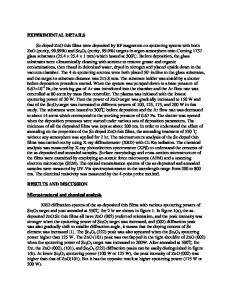
EXPERIMENT The ZnO TFTs have a bottom gate top S/D contact architecture (Fig. 1) and were fabricated on heavily p-doped 150 mm Silicon wafers (0.01 Ωcm) with 100 nm or 200 nm thermally grown SiO2 as gate oxide. The ZnO active layer was deposited at room temperature by reactive RF magnetron sputtering from a ZnO target in Ar/O2 ambient (1:1 partial pressure
Data Loading...