Effects of Zr/Ti ratio and post-annealing temperature on the electrical properties of lead zirconate titanate (PZT) thic
- PDF / 1,142,070 Bytes
- 10 Pages / 585 x 783 pts Page_size
- 84 Downloads / 763 Views
Dong-Soo Park,a) Jong-Jin Choi, Woon-Ha Yoon, and Jungho Ryu Center for Future Technology, Korea Institute of Materials Science, Changwon, Gyeong-Nam 641-010, Korea
Doh-Yeon Kimb) School of Materials Science and Engineering, Seoul National University, Gwanak-gu, Seoul 151-742, Korea (Received 6 July 2007; accepted 2 October 2007)
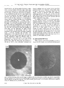
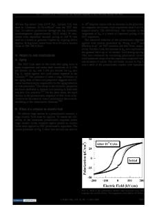
The effects of the Zr/Ti ratio on the electrical properties of lead zirconate titanate (PZT) thick films prepared by the aerosol deposition (AD) process were investigated to optimize the electrical properties of the thick film. The Zr/Ti ratio was varied among 45/55, 52/48, and 60/40, and the post-annealing temperature was varied from 500 to 900 °C. Microscopic examination of the as-deposited films revealed crack-free and dense microstructures with a thickness of 10 m. The annealed films showed markedly improved electrical properties in comparison with the as-deposited films with increasing post-annealing temperature. With increasing Zr/Ti ratio, the remnant polarization and coercive field decreased. The dielectric constant and piezoelectric coefficient, d33, were highest for the PZT 52/48 film. This film annealed at 900 °C exhibited the best overall combination of electrical properties, with a dielectric constant, remnant polarization, and piezoelectric coefficient of 1320, 31.1 C/cm2, and 150 pC/N, respectively.
I. INTRODUCTION
Lead zirconate titanate (PZT) has been widely studied for various applications in sensors, actuators, and transducers due to its excellent ferroelectric and piezoelectric properties in both bulk and film forms.1,2 Recent trends toward miniaturization and integration of electromechanical devices especially have led to development of microelectromechanical systems (MEMS). Highperformance PZT films have attracted considerable attention for their applications in MEMS.3,4 MEMS primarily comprise sensing and actuating films integrated on substrates. Preparation of dense films with excellent piezoelectric properties is therefore one of the most ima)
Address all correspondence to this author. e-mail: [email protected] b) This author was an editor of this journal during the review and decision stage. For the JMR policy on review and publication of manuscripts authored by editors, please refer to http://www. mrs.org/jmr_policy DOI: 10.1557/JMR.2008.0021 226 J. Mater. Res., Vol. 23, No. 1, Jan 2008 http://journals.cambridge.org Downloaded: 14 Mar 2015
portant parameters for MEMS applications. Conventional fabrication techniques for PZT films can be divided into two categories: thin and thick film technology. The sol-gel method is a popular technique for PZT thin films because of the resultant film’s excellent electrical properties and low processing temperature. However, it is difficult to obtain PZT films >1 m thick by a single coating process. Although a multiple coating method can be used to increase film thickness up to 10 m, interlayer cracks are likely to occur in the resultant film.5 Recently, there has been an increased interest in PZT thick films. Thick f
Data Loading...