Electric Field Induced Patterning of Polymer Films
- PDF / 203,694 Bytes
- 6 Pages / 612 x 792 pts (letter) Page_size
- 49 Downloads / 364 Views
Electric Field Induced Patterning of Polymer Films.
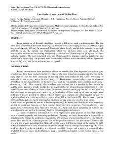
David G. Bucknall and G. Andrew D. Briggs Department of Materials, Oxford University, Parks Road, Oxford, OX1 3PH, U.K. ABSTRACT By confining a polymer film between two electrodes one of which is solid but thin enough to be flexible, a characteristic lateral morphology is produced when a strong electric field is applied across the film. A simple model to describe the observed behaviour is presented which accounts for the length scales of the observed morphology. This model demonstrates that feature sizes ranging from microns to nanometers can be obtained through selective choice of key parameters. INTRODUCTION The ability to use polymers to produce patterned surfaces on a variety of length scales is of potential technological importance where cheap, large-area devices produced from nonlithographic methods are required.[1] A number of methods to achieve this have been investigated including exploitation of spinoidal dewetting of thin polymer films,[2] phase separation of polymer blends in thin films,[3-5] and diblock copolymers phase separation.[6] More recently the use of electric fields applied across unstable polymer films has produced remarkable periodic lateral structures.[7] An alternative strategy has been the use of mechanical confinement of freely standing polymer films to produce a lateral morphology which is driven by dispersion forces.[8] This paper describes the preliminary results of the stability of a thin polymer film confined between two thin capping layers, when under the influence of an electric field. The presence of a capping layer on an unstable thin polymer film such as polystyrene (PS) is known to prevent film rupture and dewetting behaviour.[9] Freely standing trilayer thin films, consisting of a homopolymer layer which has been capped on both surfaces by thin solid layers, produces a characteristic in-plane structure (lateral morphology) when annealed at elevated temperatures.[8] Similar morphology has also been observed for thin films of blends of PS and poly(methyl methacrylate) (PMMA) capped by varying thicknesses of SiOx.[5] In the present case, the morphology is not driven by either a phase separation process,[5] or an instability due to the attractive dispersion force between the capping layer-air surfaces,[8] but rather by the force between the electrodes caused by the applied electric field. EXPERIMENTAL The samples were prepared by spin coating zwitterionic telechelic polystyrene (ZT-PS) (Mw = 6.4 × 10³ g/mol, Mw/Mn = 1.05) from a dilute cyclohexanone solution (20 mg/ml) onto a silicon wafer previously sputter coated by an approximately 50 nm thick layer of aluminium. This gave a polymer layer of thickness (d) of 87 nm as determined using neutron reflection. The polymer film was vacuum dried overnight at 60 ºC and then sputter coated with another layer of Al. The Al was sputter coated onto the ZT-PS surface using a plasma coater, with a base pressure of 10-6 Y8.7.1
(a)
(b)
Figure 1: (a) Reflection mode optical micrograph of th
Data Loading...