Electrical Characterization of Laser-Irradiated 4H-SiC Wafer
- PDF / 165,781 Bytes
- 6 Pages / 612 x 792 pts (letter) Page_size
- 92 Downloads / 328 Views
Electrical Characterization of Laser-Irradiated 4H-SiC Wafer I. Salama1, N. R Quick2, A. Kar1,4, Gilyong Chung3. 1.-Laser-Aided Manufacturing, Materials and Micro-Processing Laboratory (LAMMMP), School of Optics, Mechanical, Materials, and Aerospace Engineering Department, Center for Research and Education in Optics and Lasers (CREOL), University of Central Florida, Orlando, FL 32816-2700. 2.- Applicote Associates, 894 Silverado Court, Lake Mary, FL 32746. 3.- Sterling Semiconductor, Inc. 3401 Cragmont Drive, Tampa, FL 33619. 4.- Electronic mail: [email protected]
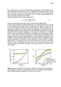
Highly conductive tracks are generated in low-doped epilayers on 4H-SiC wafers using a laserdirect write technique. The current-voltage characteristics are measured to study the effect of the applied voltage on the electric resistance and the surface contact of the irradiated tracks. The effect of multiple irradiations on the electronic properties of the fabricated tracks was investigated and compared with the effect of the conventional annealing process. A laser doping process was used to achieve n-type as well as p-type impurity doping in the substrate. The electronic properties of the doped tracks are measured and compared with those of the untreated wafers. Microstructural observation and surface analysis of the irradiated tracks are studied. Laser fabrication of rectifying contact on SiC substrates is demonstrated. INTRODUCTION SiC is superior to the conventional semiconductor materials (Si, Ge and GaAs) in many aspects that are crucial for solid state semiconductor devices. The bandgap energy in silicon carbide (Eg = 2.36 to 3.5 eV) [1] is three times that of Si and GaAs, and more than five times that of Ge. The electric field breakdown strength of SiC (3-5 MV/cm) is typically six times that of Si. Despite its higher electric field strength, the saturation electron velocity (Vsat ≈ 2 × 107 cm/s) in SiC is similar to that in GaAs. Excellent thermal conductivity of SiC (350-490 W m-1 K-1), which is three times higher than silicon and seven times higher than GaAs [1,2], allows silicon carbide to remove heat more efficiently, operate at lower internal junction temperature and therefore the cooling hardware is reduced for SiC devices. These beneficial thermal and electronic properties of SiC make it the potential candidate semiconductor for optoelectronic, high-power, temperature, -frequency, -switching speed, and radiation hard microelectronic devices where conventional semiconductor materials (e.g., Si and Ge) fail to function adequately under such conditions [1-5]. To fully utilize the above mentioned outstanding properties of SiC in high temperature and high power applications, some device building blocks (n-region, p-region, and heavily doped channels) must be fabricated. This could be a problem in SiC due to its hardness, chemical inertness, requiring the use of dry etching techniques, and the low diffusion coefficient of most impurities. A laser conversion technology, first reported by Quick as the laser directwrite technique [6-11], alters the el
Data Loading...