Electron Traps in n-GaN Grown on Si (111) Substrates by MOVPE
- PDF / 110,589 Bytes
- 6 Pages / 612 x 792 pts (letter) Page_size
- 29 Downloads / 320 Views
1068-C06-09
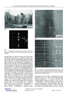
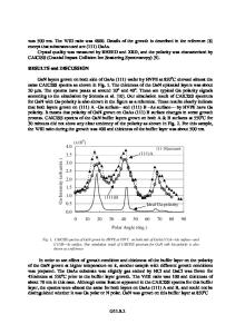
Electron Traps in n-GaN Grown on Si (111) Substrates by MOVPE Tsuneo Ito1,2, Yutaka Terada1, and Takashi Egawa1 1 Research Center for Nano-Device and System, Nagoya Institute of Technology, Gokisocho,Showa-ku, NAGOYA, 466-8555, Japan 2 DOWA Electronics Materials Co.,Ltd., Sunada 1,Iijima, AKITA, 011-0911, Japan ABSTRACT Deep level electron traps in n-GaN grown by metal organic vapor phase epitaxy (MOVPE) on Si (111) substrate were studied by means of deep level transient spectroscopy (DLTS). The growth of n-GaN on different pair number of AlN/GaN superlattice buffer layers (SLS) system and on c-face sapphire substrate are compared. Three deep electron traps labeled E2 (the energy level is not clear), E4 (0.7-0.8 eV), E5 (1.0-1.1 eV), were observed in n-GaN on Si substrate. And the concentrations of these traps observed for n-GaN on Si are very different from that observed for n-GaN on sapphire substrate. E4 is the dominant of these levels for nGaN on Si substrate, and it is not related to linear array defect like dislocation line, but it behaves like point-defect based on the analysis by electron capture kinetics, in spite of having high dislocation density to the order of 1010 cm-2. INTRODUCTION GaN and its alloys have found broad application for the visible to ultraviolet optoelectronics, high frequency, high power, and high temperature electron devices. Over a decade, the growth of these nitrides on Si substrate has become a subject of great interest, because of the numerous advantages like significantly lower cost, good thermal conductivity, and availability in large diameter. However, there are some difficulties in the growth of GaN on Si, especially cracking of GaN due to thermal mismatch between them. Recent progress of several kind of buffer layer system enables to grow 2-3 µm thick crack-free GaN layers on Si substrate [1, 2]. And using these techniques, many GaN devices on Si substrate have been demonstrated as reported by us earlier (for example; [3]). Besides, an understanding of the defects in these materials is essential for improving the material quality and device performance. Deep level transient spectroscopy (DLTS) has been used by many device researchers to characterize electronic trap states in GaN grown by MOVPE. However, currently there are no reports available on the study of deep traps in GaN grown on Si substrates. In this paper, we report electron traps in n-GaN grown on Si (111) substrates by MOVPE, and analyzed the crystal quality, electrical properties and investigated the deep traps by means of DLTS measurement. EXPERIMENT The growth of Si-doped n-GaN on 4-inch Si (111) substrate and on 2-inch c-sapphire substrate was performed by horizontal MOVPE system. The schematic diagram of these epilayer structures are shown in figure.1. In order to grow 1-µm crack-free n-GaN layers on Si substrate, we have used an i-GaN/i-AlN superlattice buffer layers system. In our experiment, two types of n- GaN on Si substrate samples were prepared. They are the growth of n-GaN on (i) 10 pairs a
Data Loading...