Microstructure of GaN Grown on (111) Si by MOCVD
- PDF / 2,822,141 Bytes
- 6 Pages / 417.6 x 639 pts Page_size
- 78 Downloads / 341 Views
igure 1. Nomarski optical micrograph showing cracking of GaN on (I 1) Si along 11 - 1001 planes.
from 20 to 100 jtm was found along 11-1001 planes, as seen in Figure 1. The layer is expected to have relaxed fully at the growth temperature, as found for GaN grown on A120 3 using in situ stress monitoring techniques [4]. The greater thermal expansion coefficient of GaN as compared to that of Si (5.6x10⁻⁶/K vs. 2.6x 10⁻⁶/K, respectively) then explains cracking since the GaN layer would be put into tension upon cooling. In spite of cracking, the GaN layer adhered to the substrate. X-ray diffraction of such layers gives (0002) GaN reflections with FWHM of 900 arcsec, similar to those found previously [2].
TEM CHARACTERIZATION OF DEFECTS IN GaN Cross-section TEM specimens were successfully prepared by usual metallographic polishing and ion milling methods for both [110] and [1-12] Si orientations in spite of the cracking. Cracks were found passing directly across the layer and into the Si substrate. The cracks were open with no indication of subsequent deposition, consistent with their forming after growth [1]. No evidence of de-adhesion of the layer from the substrate was seen where the cracks cross the interface into the Si. The GaN layer was found to be single phase and with no 30°-misoriented grains as seen in other material grown by molecular beam epitaxy (MBE) [5]. Selected-area diffraction demonstrated the epitaxial orientation seen previously for GaN on (11l) Si [2,3,5]: (0001) 11(111)
interface plane
[1-100] II[11-2]
direction in plane "
[11-20] II[1-10]
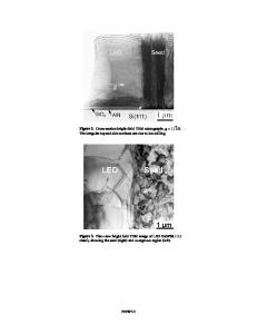
Dislocations thread from the buffer layer to the surface of the GaN layer along the c-axis, growth direction. Examination in cross-section with different diffracting beams can be used to determine the Burger's vectors of individual dislocations, which for hexagonal close-packed lattices are [6]: a (or 1/3, in the basal lattice plane), c (, along the hexagonal axis), or a+c (1/3, mixed character). In Figure 2, image (a) uses the (0004) reflection to illuminate the cores of dislocations with Burger's vectors having a c-axis component. Image (b) uses (1-100) to image those with a basal plane component. Detailed examinations with several reflections indicate that almost all dislocations are detected in Figure 2b) and have a basal-plane component. Those with a c-axis component seen in Fig. 2a (-1/3 of the total) are almost all of mixed character. The additional ones in Fig. 2b (-2/3 of the total) have purely basal-plane Burger's vectors, b = a; since the dislocation lines are fairly straight along the c-axis, these are edge dislocations. Very few dislocations have b = c corresponding to pure screw character. This distribution of Burger's vectors is like that found by us [7] and others [8] in GaN on sapphire.
Figure 2. Weak-beam TEM images obtained near [11-20] orientation, a) g = (0004), with cores of dislocations having b = a + c illuminated. b) g = (1-100), with cores of all dislocations illuminated. A crack running through the layer and into the Si substrat
Data Loading...


