Electronic Properties of Hot-Wire Deposited Nanocrystalline Silicon
- PDF / 385,912 Bytes
- 6 Pages / 414.72 x 648 pts Page_size
- 17 Downloads / 321 Views
ABSTRACT We compare the electronic properties of nanocrystalline silicon from hot-wire chemical vapor deposition in a high-vacuum and an ultra-high-vacuum deposition system, employing W and Ta as filament material. From the constant photocurrent method we identify a band gap around 1.15 eV while, in contrast, a Tauc plot from optical transmission data guides to a wide band gap above 1.9 eV. The sudden change-over from nanocrystalline to amorphous structure in a hydrogen dilution series is also find in the dark and photoconductivity measurements. The samples show a metastability effect in the dark conductivity upon annealing in vacuum with an increase in the dark conductivity, with the large dark conductivity decreasing slowly after the annealing cycle when the cryostat is flushed with air. We identify larger values for the mobility-lifetime products, which corresponds to the smaller defect density shoulder in constant photocurrent spectra, for the ultra-high-vacuum deposited material compared to the high-vacuun counterpart.
INTRODUCTION The detailed knowledge of the electronic properties of nanocrystalline silicon (nc-Si) is important from a fundamental point of view and also for any application in devices such as solar cells. We report on a study on the properties of nc-Si from hot-wire chemical vapor deposition (HWCVD) which we deduce from dark and photocurrent measurements. We focus on a comparison between samples from a high-vacuum (HV) and an ultra-high-vacuum (UHV) deposition system and a hydrogen dilution series from the latter. 600
500 S400
.
50
.
,
.
.
o (b)
(a)40
".2E 300
E 30 -
." 200
~100
20 10 0
0
1.8
.
2.0
2.2
2.4
energy Ep. (eV)
2.6
2.8
i
,
0.6
0.8
1.0
1.2
1.4
1.6
1.8
2.0
energy EPh(eV)
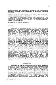
Figure 1: Wide band gap E"' of 1.97 eV from a Tauc plot (a) and identification of the band gap identical to that of c-Si from CPM-spectra at smaller energies (b).
921 Mat. Res. Soc. Symp. Proc. Vol. 507 © 1998 Materials Research Society
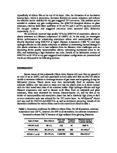
EXPERIMENTAL Samples were deposited in a high vacuum (HV) and an ultra-high-vacuum 25000 • , • , . . . . . . . (UHV) hot-wire CVD deposition system 20000 SiHl4 for which Refs. [1,2] gives more details. °, / • flow rate C Standard parameters in the study here °%) /A (sccm) 15000 for the HV and UHV deposition are tungsten as filament material with 250 pm in 66 ._ 28 .73 diameter and a filament temperature of 5 , J , J , .C 0 about 1650'C. In a modification of the UHV set-up tantalum served as filament material with a 380 pm thick wire. 420 440 460 480 500 520 540 560 580 We investigate a hydrogen dilution AV(cm") series from the UHV deposition system with a deposition temperature of 2000C where the hydrogen gas flow rate was Figure 2: Comparison of Raman spectra for fixed at 60 sccm and the silane gas flow the hydrogen dilution series shows a small rates were set to 2, 4, 6, and 8 sccm. The gradual change in crystalline fraction X, unhydrogen dilution ratio D is defined by til at a dilution of D = 7.5 the films become D = [H2 ]/[SiH4]. There is no g
Data Loading...