Electrostatic Force Microscopy of Nanofibers and Carbon Nanotubes: Quantitative Analysis Using Theory and Experiment
- PDF / 961,883 Bytes
- 6 Pages / 612 x 792 pts (letter) Page_size
- 97 Downloads / 390 Views
1025-B13-03
Electrostatic Force Microscopy of Nanofibers and Carbon Nanotubes: Quantitative Analysis Using Theory and Experiment Sujit Sankar Datta1, Cristian Staii1,2, Nicholas J. Pinto3, Douglas R. Strachan1,4, and AT Charlie Johnson1 1 Department of Physics and Astronomy, University of Pennsylvania, Philadelphia, PA, 19104 2 Department of Physics, University of Wisconsin, Madison, Madison, WI, 53706 3 Department of Physics and Electronics, University of Puerto Rico, Humacao, 00791-4300, Puerto Rico 4 Department of Materials Science and Engineering, University of Pennsylvania, Philadelphia, PA, 19104 ABSTRACT Electrostatic force microscopy (EFM) is a widely used scanning-probe technique for the characterization of electronic properties of nanoscale samples without the use of electrical contacts. Here we review the basic principles of EFM, developing a quantitative framework by which EFM measurements of extended nanostructures can be understood. We support our calculations with experimental data of EFM of carbon nanotubes and conducting or insulating electrospun polyaniline-based nanofibers. Furthermore, we explore routes towards extending EFM as a means of non-invasively probing the local electronic density of states of carbon nanotubes.
INTRODUCTION Scanning probe techniques are crucial to fundamental studies of structure and properties at the nanoscale. Electrostatic force microscopy (EFM) has found wide applicability as a means of non-invasively probing various electronic properties of nanostructures in its various forms. In particular, phase-EFM (also referred to as Scanning Conductance Microscopy, heretofore simply referred to as ‘EFM’) can be used to characterize conducting and dielectric nanostructures via the capacitive coupling between the nanostructure and a conducting tip, biased with a specific voltage. EFM operates in a two-pass mode: in the first pass, the atomic force microscopy (AFM) tip is unbiased, mapping out the sample topography in ‘tapping mode’. After the first pass, the AFM tip is raised up to a controllable height h above the sample, biased with a fixed voltage (Vtip), and retraces the sample topography (figure 1) while being driven at resonance. In this second pass, the phase shift of the cantilever oscillation is monitored as the sample is mapped out.
Vtip
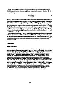
Figure 1. Schematic showing the two passes of EFM: (left) unbiased tip acquires sample topography; (right) biased tip is raised to a specified height above the sample and retraces sample topography. Modeling the AFM cantilever in the second-pass (interleave mode) as a harmonic oscillator, the capacitive coupling between the tip and the sample leads to a phase shift given by [1]: Φ(x, y) = −
Q ∆C"(h)∆V 2 2k
(1)
where Q is the cantilever quality factor, k is the cantilever spring constant, ∆C"(h) is the second derivative of the difference between the tip-sample capacitance and the tip-substrate capacitance as a function of the lift height h, and ∆V is the difference between the tip bias voltage and the sample surface electrostati
Data Loading...


